
 Shopping Cart
2
Shopping Cart
2


 Smart Quote
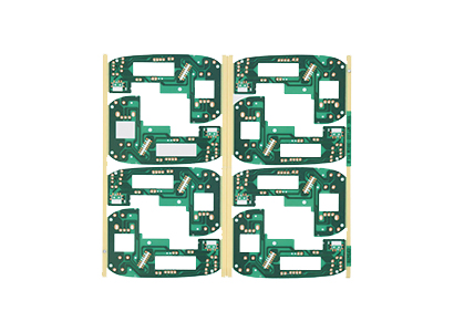
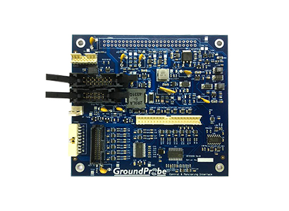


For electronics projects, professional pcb assembly services turn a fabricated printed circuit board into a functional electronic assembly. The work can include design-file review, component preparation, solder paste printing, automated component placement, through-hole insertion, soldering, inspection, testing and anti-static packing.
Successful PCBA production depends on more than placing components on a board. Gerber files, the bill of materials, pick-and-place data, assembly drawings and testing instructions must all refer to the same approved revision. This guide explains what PCB assembly normally includes, how SMT and through-hole processes differ, what files are required for quotation and which quality checks should be discussed before production.
What PCB Assembly Services Usually Include
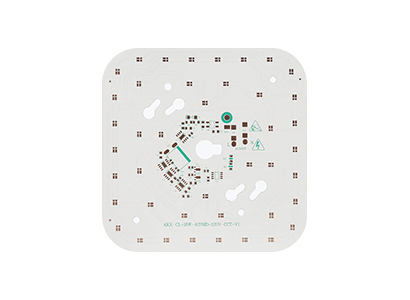
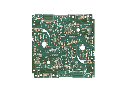
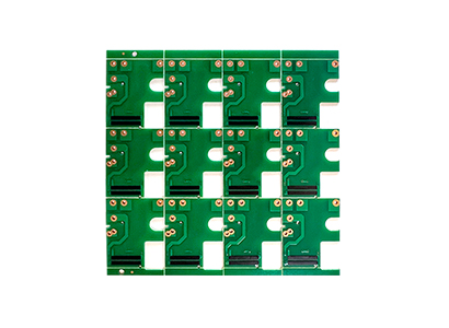
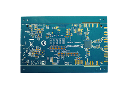
PCB assembly is the process of mounting electronic components on a fabricated circuit board and creating reliable electrical and mechanical connections. A complete service usually begins before the first component reaches the placement line. The technical team first checks whether the fabrication data, BOM, placement coordinates and assembly notes are consistent.
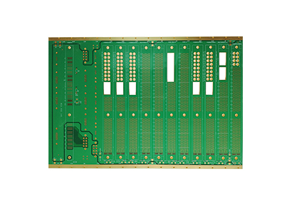
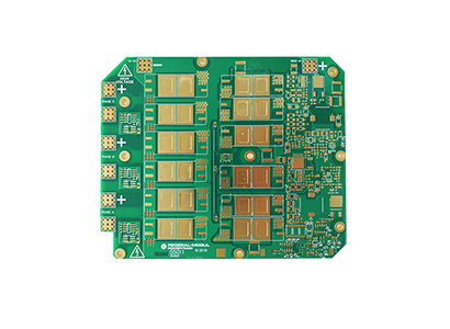
The assembly route is then planned according to the component mix. A compact control board may rely mainly on surface-mounted devices, while a power or industrial board may also require terminal blocks, relays, transformers, connectors and other through-hole components. Double-sided boards and mixed-technology designs require additional planning for soldering order, part height and inspection access.
Component sourcing may also be included when complete manufacturer part numbers and approved alternatives are provided. Clear sourcing data is important because two components with similar values may still have different packages, footprints, current ratings, tolerances or pin configurations.
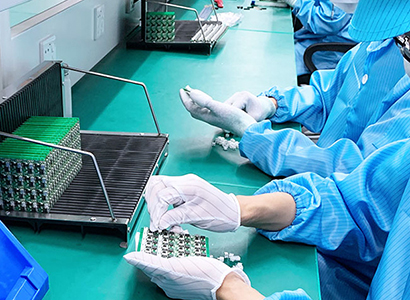
After assembly, the boards may move through visual inspection, automated optical inspection, electrical checks, functional testing and packing. The exact scope should be agreed before production because a basic visual review is different from firmware programming or a full function test under a defined load.
A Typical PCBA Service Scope
- Gerber, drill, BOM, placement and assembly drawing review.
- Solder paste printing and automated SMT component placement.
- Reflow soldering for surface-mounted components.
- Through-hole insertion and soldering for connectors and larger parts.
- Mixed SMT and through-hole assembly on the same board.
- Visual inspection, AOI, X-ray or other checks when applicable.
- Electrical or functional testing based on supplied procedures.
- Labeling, anti-static packing and shipment preparation.

PCB Manufacturing vs PCB Assembly
Bare PCB manufacturing creates the unassembled circuit board. It forms the copper circuitry, drilled holes, plated vias, solder mask, silkscreen, surface finish and finished board outline. Its main concerns include material selection, stack-up, copper thickness, hole structure, impedance requirements and dimensional tolerances.
PCB assembly begins when electronic components are mounted on the fabricated board. The output is a populated printed circuit board assembly, commonly called a PCBA. Assembly quality depends on both the bare board and the component data, so the two stages should not be treated as unrelated processes.
For example, an incorrect footprint can prevent a component from fitting correctly even when the bare PCB itself passes fabrication inspection. Likewise, a misplaced polarity mark or inaccessible test point can make assembly, inspection and debugging more difficult.
| Item | Bare PCB Manufacturing | PCB Assembly / PCBA |
| Main output | An unassembled printed circuit board. | A populated board with installed electronic components. |
| Core files | Gerber, drill data, stack-up, board outline and fabrication notes. | Gerber, BOM, pick-and-place data, assembly drawing and test instructions. |
| Main process | Lamination, drilling, plating, imaging, etching, solder mask and finishing. | Component placement, soldering, inspection, testing and packing. |
| Common risks | Stack-up mismatch, hole error, open circuit, short circuit or outline issue. | Wrong component, polarity error, solder bridge, poor joint or test failure. |
Revision control is especially important when PCB fabrication and assembly are ordered together. Gerber files, the BOM and placement data should all carry the same revision name. If different file versions are mixed, production should pause until the correct set is confirmed.
SMT, Through-Hole Assembly and BOM Preparation
Surface-Mount Technology
Surface-mount technology, or SMT, places components directly on solder pads on the PCB surface. It is widely used for chip resistors, capacitors, diodes, LEDs, integrated circuits and compact electronic modules. SMT supports dense layouts and repeatable automated production.
A typical SMT process includes solder paste printing, solder paste inspection, pick-and-place mounting, reflow soldering and post-reflow inspection. The process settings depend on the solder paste, component package, thermal mass, board design and required quality level.
Through-Hole Technology
Through-hole technology, or THT, inserts component leads through plated holes in the PCB. It is commonly used for connectors, terminal blocks, relays, transformers, switches and larger capacitors. These parts may be inserted manually or with dedicated equipment before wave, selective or manual soldering.
Some manufacturers informally use the term “DIP assembly” for through-hole work. Technically, however, DIP means dual inline package and describes a specific package style. THT is the more accurate term for the overall through-hole assembly process.
SMT Is Commonly Used For
- Compact and high-density board layouts.
- Chip resistors and capacitors.
- ICs, diodes, LEDs and small packages.
- Automated double-sided assembly.
- Repeatable medium- and higher-volume placement.
THT Is Commonly Used For
- Connectors and terminal blocks.
- Relays, switches and transformers.
- Large capacitors and heavier components.
- Parts exposed to mechanical stress.
- Mixed-technology industrial and power boards.
Why the BOM Is Critical
The bill of materials identifies every component required for the assembly. A production-ready BOM should include reference designators, manufacturer names, manufacturer part numbers, package information, values, quantities, tolerances, electrical ratings and approved alternatives.
A description such as “10K resistor” is not sufficient because the package size, tolerance and power rating remain unclear. An IC should also be listed by its complete manufacturer part number because similar product names can have different packages, temperature ranges or pinouts.
Optional and no-mount parts should be clearly marked. If substitutions are allowed, the approved conditions should be stated instead of leaving the production team to choose an alternative without authorization.
Recommended BOM Fields
- Reference designator, such as R1, C4, U2, D3 or J1.
- Manufacturer and full manufacturer part number.
- Package, value, tolerance and voltage or current rating.
- Quantity per board and total required quantity.
- Approved alternatives and substitution restrictions.
- No-mount, optional and customer-supplied component notes.
- Special storage, programming or installation requirements.
How a PCBA Project Moves Through Production
Although each board has different technical requirements, most PCB assembly projects follow the same general workflow. The first stage is file review. Engineers compare the Gerber files, BOM, coordinate data and drawings to identify missing information, revision conflicts or footprint concerns.
Once the files are approved, bare boards, stencils and components are prepared. Moisture-sensitive devices may require controlled storage or baking according to their handling condition. SMT parts are then mounted and reflow soldered before through-hole components are inserted.
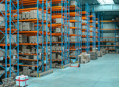
Inspection and testing follow assembly. Approved boards are labeled and packed using suitable anti-static protection. Any special tray, separator, barcode, packaging or shipment requirement should be confirmed before the order enters production.
| Stage | Main Work | Purpose |
| 1. File review | Check PCB data, BOM, coordinates and assembly notes. | Identify missing or conflicting information before production. |
| 2. Material preparation | Prepare boards, stencil, components and process documents. | Support stable placement and soldering. |
| 3. SMT assembly | Print solder paste, mount components and perform reflow. | Install compact surface-mounted components. |
| 4. THT assembly | Insert and solder connectors, terminals and larger parts. | Complete mixed-technology assemblies. |
| 5. Inspection and test | Review placement, soldering, polarity and required functions. | Confirm the assembly meets agreed acceptance criteria. |
| 6. Packing | Apply labels and anti-static protection. | Protect completed boards during storage and shipment. |
PCB Assembly Testing and Quality Control
The inspection plan should match the board design, production stage and end-use requirements. Prototype boards may focus on basic design verification, while repeated batch production requires controlled inspection standards and documented pass-fail criteria.
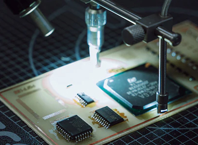
Visual inspection checks component presence, polarity, orientation, solder bridges, damaged components and obvious soldering defects. Automated optical inspection can improve repeatability by comparing component placement and visible solder conditions against programmed inspection data.
X-ray inspection may be considered for hidden solder joints such as BGA or bottom-terminated packages when the board design and project requirements justify it. Electrical testing can check continuity, shorts or defined test points, while functional testing verifies whether the assembled board performs its intended operation.
Many electronics projects use IPC-A-610: Acceptability of Electronic Assemblies as a reference for electronic assembly acceptance. The required class and inspection criteria should still be confirmed according to the product application and project agreement.
Functional testing cannot be defined by a general request such as “test every board.” The supplier needs the input voltage, firmware version, connection method, fixture details, expected output, load condition and pass-fail limits. Providing this information early helps avoid quotation changes after assembly has started.
Visual Inspection
Checks missing parts, polarity, orientation, solder bridges, damaged pads and visible soldering issues.
AOI and X-Ray
Supports repeatable inspection of visible placement and, when required, hidden solder-joint conditions.
Functional Testing
Confirms defined board functions using supplied firmware, fixtures, instructions and acceptance limits.

Files Required for a PCBA Quotation
A complete RFQ allows the technical team to review both PCB fabrication and component assembly. The latest Gerber package should define the board structure, while the BOM and placement data should identify what must be installed and where each component belongs.
Pick-and-place data normally includes reference designators, X and Y coordinates, rotation and mounting side. Assembly drawings provide additional visual guidance for polarity, connector direction, optional parts, mechanical restrictions and special soldering requirements.
Test and programming files should be supplied whenever these services are required. The quotation should also state the prototype or batch quantity, PCB material, layer count, copper weight, surface finish, panel requirement and packaging expectations.
PCBA RFQ Checklist
- Gerber and drill files: Complete PCB fabrication data for the approved revision.
- BOM: Manufacturer part numbers, packages, quantities and substitution rules.
- Pick-and-place file: Coordinates, rotation, board side and reference designators.
- Assembly drawing: Polarity, connector direction, no-mount parts and special notes.
- PCB requirements: Material, layer count, thickness, copper weight and surface finish.
- Quantity: Prototype, engineering validation, pilot run or batch quantity.
- Testing instructions: Test steps, fixtures, firmware and pass-fail limits.
- Packing requirements: Labels, barcodes, trays, separators and anti-static packaging.
Factors That Affect PCBA Cost and Lead Time
A PCB assembly quotation includes more than a component placement fee. Bare-board complexity, component availability, package type, assembly side, soldering method, inspection depth and testing requirements all influence production planning.
Fine-pitch ICs, BGA packages, very small passive components and dense double-sided layouts usually require tighter process control. Large through-hole components can add manual insertion or selective soldering work. Consigned components may also need incoming verification, counting and special handling.
Component sourcing can become a major schedule factor when a specified part has a long manufacturer lead time or limited availability. Providing approved alternatives early gives the sourcing team more options without creating unauthorized substitutions.
| Factor | What to Confirm | Possible Effect |
| PCB complexity | Layer count, material, copper, vias, finish and panel design. | Changes fabrication cost and production preparation. |
| Component packages | Pitch, package size, BGA, polarity and mounting side. | Changes placement, inspection and process-control needs. |
| Component sourcing | Availability, approved brands, alternatives and supplied parts. | Can significantly affect price and delivery time. |
| Assembly method | Single-sided, double-sided, SMT, THT or mixed assembly. | Changes stencil, reflow, insertion and soldering work. |
| Testing scope | Visual, AOI, X-ray, electrical, programming or functional test. | Changes fixtures, engineering preparation and test time. |
| Order quantity | Prototype, pilot run or regular batch production. | Affects setup allocation, material purchasing and unit cost. |
Design Details That Support Reliable Assembly
Assembly quality begins during PCB design. Correct land patterns help components align with their solder pads, while suitable component spacing improves placement, soldering and inspection. Footprints should be checked against the exact package listed in the BOM rather than a general component description.
Clear polarity and pin-one markings reduce interpretation risk for diodes, electrolytic capacitors, LEDs, ICs and connectors. Fiducial marks can support automated alignment, especially on boards with fine-pitch devices or dense component placement.
Accessible test points can simplify electrical testing, firmware programming and debugging. They should be designed around the actual test method, fixture and probe access rather than added without a defined purpose.
Assembly-Friendly Design Checks
- Match every PCB footprint with the selected component package.
- Provide sufficient clearance around connectors and tall components.
- Mark polarity and pin-one direction clearly.
- Use suitable fiducials for automated placement.
- Provide accessible test and programming points where needed.
- Confirm double-sided assembly and reflow limitations.
- Use consistent revision names across all production files.
Prototype PCB Assembly vs Batch Production
Prototype assembly is normally used to verify circuit function, component footprints, connector orientation, mechanical clearance and basic firmware operation. Findings from the prototype stage may lead to changes in the PCB layout, BOM, enclosure or test procedure.
Batch production focuses on repeatability. Once the design is stable, the approved revision, component substitution rules, inspection criteria, test instructions, labeling and packaging requirements should be controlled.
A pilot run can provide a useful transition between prototype and full production. It allows the assembly process and test method to be evaluated using a limited quantity before larger material commitments are made.
Prototype Focus
- Verify circuit function.
- Check footprints and polarity.
- Confirm connector fit.
- Review test-point access.
- Identify design changes.
Batch Production Focus
- Control the approved revision.
- Maintain the confirmed BOM.
- Standardize inspection.
- Use repeatable test procedures.
- Confirm labeling and packaging.
Projects That May Require PCB Assembly Services
PCBA services are suitable for projects that already have electronic design data and need physical boards for prototype validation, pilot production or regular manufacturing. Common examples include industrial control boards, communication modules, sensor products, instrumentation, lighting controls, smart devices and power electronics.
Projects for medical, automotive, aerospace or other regulated applications may require additional certification, documentation, traceability, material control and testing. These requirements should be identified during quotation rather than assumed from the general product category.
PCB Assembly Services FAQ
What are PCB assembly services?
PCB assembly services turn a fabricated PCB into a populated electronic assembly. The scope may include file review, component sourcing, SMT placement, through-hole insertion, soldering, inspection, testing, programming, labeling and packing.
What is the difference between PCB and PCBA?
A PCB is the unassembled circuit board. A PCBA is the completed board after electronic components have been mounted and soldered.
What files are needed for a PCBA quotation?
The main files are Gerber data, drill files, a complete BOM, pick-and-place coordinates and assembly drawings. Testing instructions, firmware, PCB specifications, quantity and packing requirements should also be included when applicable.
How does SMT differ from through-hole assembly?
SMT mounts components directly on surface pads and is suitable for compact automated assembly. Through-hole technology inserts leads through plated holes and is commonly used for connectors, terminals, relays and larger components.
Can SMT and through-hole components be used on the same PCB?
Yes. Mixed assembly is common on control, power and industrial boards. The production plan should account for component height, soldering order, thermal sensitivity and inspection access.
What affects a PCB assembly quotation?
Important factors include PCB complexity, component quantity, package type, sourcing availability, single- or double-sided assembly, through-hole work, inspection requirements, testing depth, order quantity and packaging.
Send Your PCBA Files for Technical Review
Reliable PCB assembly starts with complete and consistent production data. Before requesting a quotation, confirm that the Gerber files, BOM, pick-and-place data and assembly drawings all use the same approved revision.
Include the required quantity, PCB specifications, component sourcing preferences, testing instructions and packing requirements. Clear information helps the manufacturing team evaluate the PCB fabrication and assembly scope more accurately.


