
Time:2026-06-29 Views:
In compact electronics, an hdi pcb design must solve routing density, signal stability, layer transitions, soldering quality, and production reliability at the same time. Therefore, blind vias, buried vias, microvias, stackup design, via filling, surface finish, and testing requirements should be reviewed before fabrication begins.
Article Navigation
A dense PCB project usually starts with a simple goal: place more functions into less space. However, the real challenge is not only smaller board size. The board must still support stable electrical performance, reliable solder joints, practical fabrication, and clear inspection requirements.
For this reason, HDI board manufacturing should be planned early. A finished layout may look correct in CAD software, but small choices in via structure, stackup, copper thickness, pad design, and material can affect production. This guide explains how HDI structures work and what project information should be prepared before manufacturing review.
HDI means high-density interconnect. In PCB manufacturing, it refers to a board structure that uses finer traces, smaller vias, tighter spacing, and more compact layer connections than a standard pcb circuit board. As a result, more signals can be routed inside a smaller board outline.
However, HDI is not just a visual upgrade. It is a manufacturing structure that supports fine-pitch components, short signal paths, compact power distribution, and dense assembly layouts. Therefore, the design must match both electrical requirements and fabrication process limits.
In many projects, HDI becomes necessary when through-hole vias consume too much routing space. A through-hole via passes from the top layer to the bottom layer. Because of that, it can block routing channels on inner layers that do not need the same connection.
By contrast, blind vias, buried vias, and microvias connect only the required layers. This gives dense boards more routing freedom. Meanwhile, it also increases the need for accurate stackup planning, drilling control, plating quality, and lamination review.
Via structure is the heart of HDI board design. A via is a plated connection between copper layers. However, each via type has a different layer span, process route, and manufacturing risk. Therefore, via selection should be based on the layout problem it solves.
A blind via starts from an outer layer and stops at an inner layer. A buried via connects internal layers only. A microvia is a very small via, usually formed by laser drilling. In a blind buried via pcb project, these structures may work together to reduce routing congestion and keep surface layers open for components.
| Via Type | Layer Connection | Typical Use | Main Check |
| Blind via | Outer layer to inner layer | Escapes dense surface components without passing through all layers | Depth, pad size, registration, plating, layer pair |
| Buried via | Inner layer to inner layer | Keeps outer layers open for pads, components, and routing | Lamination sequence, drilling, plating, inspection access |
| Microvia | Short buildup layer span | Supports fine-pitch BGA fanout and compact layer transition | Laser drilling, capture pad, filling, reliability |
| Via-in-pad | Via placed inside a solder pad | Saves fanout space under fine-pitch packages | Filling, capping, pad flatness, soldering quality |
First, blind vias help surface components reach inner layers without drilling through the full board. This saves space on layers that do not need the same connection. In addition, blind vias can reduce unnecessary via stubs in some high-speed layouts.
However, blind via depth must remain practical. A deep blind via can create plating difficulty when the dielectric span is too thick for the selected hole size. Therefore, the hole diameter, pad diameter, dielectric thickness, copper requirement, and layer pair should be reviewed together.
Next, buried vias connect internal layers without appearing on the board surface. This keeps the top and bottom sides cleaner for solder pads, test points, connectors, and fine component placement. As a result, buried vias can improve routing freedom in dense internal layers.
At the same time, buried vias require additional manufacturing steps. The internal layers must be drilled, plated, inspected, and laminated before the full board stack is completed. Therefore, buried vias should be used where they solve a clear routing or structure problem.
Microvias are small laser-drilled vias used for short layer transitions. They are common around fine-pitch BGA packages, memory devices, compact modules, RF sections, sensors, and control boards. Because they occupy less space, microvias can make routing possible where mechanical vias are too large.
Nevertheless, microvia reliability depends on drilling quality, plating, pad design, filling method, and thermal stress. Stacked microvias can save space, but they need stronger reliability review. Staggered microvias may use more area, yet they often provide better manufacturing margin.

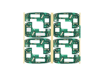
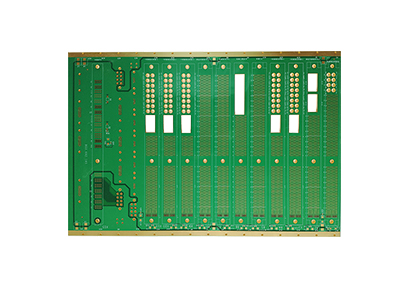
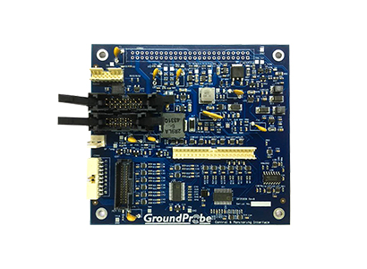
This HDI board example supports dense layer transitions, fine routing, and compact electronic product design.
View HDI Board
Fine pads, compact routing, and microvia structures should be reviewed before production release.
Check HDI CapabilityCompact electronic products often combine processors, memory, sensors, wireless modules, displays, connectors, charging circuits, and power management inside a limited enclosure. Therefore, the board must provide more interconnections without increasing the outline size.
In addition, fine-pitch packages leave very little fanout space. A standard through-hole via may not fit between pads. In that case, microvias and via-in-pad structures help signals move into inner layers with shorter routing paths.
Moreover, high-speed signals need controlled reference planes, clear return paths, and stable impedance. HDI routing can reduce long detours, but it cannot replace good signal planning. Therefore, differential pairs, clock lines, RF traces, and sensitive analog routes still require careful layout rules.
For communication devices, medical electronics, automotive modules, industrial controllers, IoT devices, compact computing boards, and handheld instruments, HDI structures can support smaller boards and higher functional density. However, each project should confirm whether the added process complexity is justified by the actual routing requirement.
HDI board technology is most useful when standard multilayer routing no longer provides enough space or performance margin. Therefore, it should be selected for a clear engineering reason, not only because the product is small.
The following project types are usually strong candidates for HDI manufacturing review. In these cases, compact layout, fine-pitch assembly, signal control, and layer transition quality can directly affect the final product.
Useful for compact RF, antenna, wireless, and high-speed signal layouts where controlled routing matters.
Suitable for small instruments, monitoring devices, and sensor boards with dense components and stable interconnect needs.
Helpful when compact modules need strong routing control, clear documentation, and reliability-focused review.
Useful for dense controllers, compact I/O boards, power management sections, and multi-signal routing designs.
Stackup planning defines how copper layers, dielectric materials, vias, and buildup layers connect. Therefore, it affects drilling, lamination, impedance, soldering, and inspection. A layout finished without a confirmed stackup may need heavy rework later.
A multilayer hdi pcb can use different buildup structures. Common examples include 1+n+1 and 2+n+2 designs. The “n” represents the core layers, while the numbers on both sides represent buildup layers. However, the correct structure depends on component pitch, routing density, board thickness, and reliability needs.
| Structure | Typical Meaning | When It May Fit |
| 1+n+1 | One buildup layer on each side of the core | Moderate HDI density, outer-layer microvia fanout, compact but practical routing |
| 2+n+2 | Two buildup layers on each side of the core | Higher component density, more complex layer transitions, limited board outline |
| Any-layer HDI | Advanced microvia connections across multiple layers | Very dense modules where simpler structures cannot meet routing needs |
In addition, stackup affects controlled impedance. Dielectric thickness, copper thickness, trace width, spacing, and material properties all work together. Therefore, impedance targets should be confirmed before final routing, especially for high-speed digital and RF sections.
IPC/JPCA-2315 is a useful external reference for HDI and microvia design structures. It discusses HDI design rules, material selection, and microvia technologies. Therefore, engineering teams can also use IPC HDI design guidance as a standards-based reference when defining documentation and design expectations.
Before fabrication, HDI projects need practical DFM review. DFM means design for manufacturability. In other words, it checks whether the board can be built with stable process margins, not only whether the circuit appears correct in design software.
The review should cover layer order, via span, drill size, pad size, annular ring, copper weight, solder mask clearance, impedance, surface finish, and testing needs. Moreover, fabrication notes should state each special requirement clearly.
First, every blind via and buried via should match the intended layer pair. A note that only says “blind via” is not enough. Instead, the stackup drawing and drill files should show the actual connection span, such as L1-L2 or L2-L5, depending on the design.
Next, the annular ring must allow drilling and layer alignment tolerance. The annular ring is the copper area around a drilled hole. If it is too small, registration shift can reduce connection quality. Therefore, dense routing should not remove all manufacturing margin.
Via filling becomes important when vias sit inside solder pads. Open vias can pull solder into the hole during assembly. As a result, solder joints may lose volume or become uneven. Therefore, via-in-pad designs often need filling and capping, depending on component pitch and assembly requirements.
Material selection affects drilling, lamination, impedance, thermal behavior, and soldering. Standard FR-4 may support many projects, while high-speed, RF, high-temperature, or mixed-material boards may need different laminates. Therefore, material choice should follow the operating environment and electrical requirements.
Copper weight also needs review. Thin copper helps fine-line etching, while heavier copper supports current and heat spreading. However, heavy copper can make fine spacing harder to produce. Therefore, copper weight should match both signal density and power requirements.
Surface finish affects pad flatness, solderability, storage, and fine-pitch assembly. ENIG, HASL, OSP, immersion silver, and other finishes serve different needs. Therefore, the correct finish depends on component pitch, assembly process, storage plan, and project requirements.
Finally, testing requirements should be stated before production. Electrical testing, impedance testing, visual inspection, microsection requests, and other acceptance checks depend on the project. Therefore, they should not be assumed without written requirements.

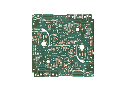
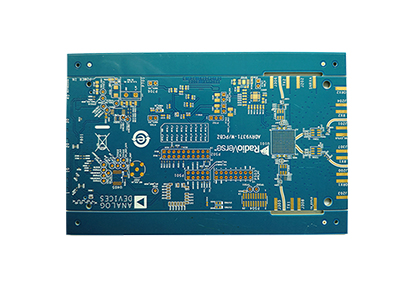
Layer pair, drilling method, pad size, and lamination sequence should be checked before fabrication.
Review HDI Board Page
Stackup, copper weight, surface finish, and testing requirements should be aligned before quotation.
View Product CategoryHDI fabrication and PCB assembly are closely connected. Therefore, a board that can be fabricated may still create soldering risk if the pad design, via-in-pad rules, solder mask clearance, or surface finish do not match the assembly process.
For fine-pitch BGA components, via filling and pad flatness are especially important. Open holes inside solder pads can absorb solder during reflow. Because of that, filled and capped via-in-pad structures may be required for reliable solder joints.
Stencil design also matters. Small pads need controlled paste volume, while larger power pads may need enough solder for thermal and mechanical stability. Therefore, BOM data, placement files, paste layers, and assembly drawings should align with fabrication files.
In addition, thermal balance should be reviewed. Dense copper areas and small signal pads heat at different rates during reflow. As a result, copper distribution, component mass, panel design, and reflow requirements can influence assembly quality.
A clear RFQ helps avoid repeated questions and uncertain pricing. Therefore, the project package should separate required data from optional preferences. Required data includes the design files, layer count, material, copper weight, surface finish, quantity, and testing requirements.
In addition, special requirements should be written clearly. If a via needs filling, capping, plugging, or copper filling, the note should identify the exact via group. If controlled impedance is required, the target value and trace group should be included.
Moreover, PCBA projects should include BOM, pick-and-place file, assembly drawing, paste layer, polarity notes, and testing request. When the BOM contains hard-to-source parts, approved alternatives can also reduce review time.
An inquiry can be sent when the design direction is clear enough for engineering review. However, early review does not require every detail to be locked. Preliminary Gerber data, expected layer count, main component pitch, and via structure notes can help identify manufacturing risks before the layout becomes difficult to change.
For quotation and production planning, complete data is needed. Therefore, the package should include fabrication files, assembly files if PCBA is required, quantity, material, surface finish, testing requirements, and special notes. Incomplete data may lead to repeated questions or unclear quotation scope.
The following PCBXINSHUN pages support further manufacturing review. They connect this technical guide with related product capability, assembly support, and project communication.
Review HDI board examples, blind hole structures, and high-density interconnect board references.
Open HDI Board Page →Check PCB manufacturing capability information before sending complex board requirements.
View Capabilities →Review PCBA support when the project includes SMT assembly, BOM handling, and testing needs.
Open Assembly Page →Blind vias connect an outer layer to an inner layer. Buried vias connect internal layers only and do not appear on the board surface. Therefore, both structures help save routing space and reduce unnecessary through-hole connections in dense layouts.
A microvia is a small via, usually created by laser drilling. It is commonly used for short layer transitions around fine-pitch components. However, microvia pad size, filling method, stacking choice, and reliability requirements should be reviewed before production.
It is used when dense components, compact outlines, high-speed routing, or limited layer space require more advanced interconnects. The structure may include blind vias, buried vias, microvias, sequential lamination, and controlled impedance routing, depending on project requirements.
The project package should confirm Gerber files, drill files, layer count, stackup, material, copper weight, surface finish, quantity, and testing requirements. If assembly is included, BOM, pick-and-place data, paste layers, and assembly drawings should also be provided.
No. Some compact boards can still use standard multilayer structures. However, fine-pitch components, routing congestion, via-in-pad requirements, controlled impedance, or strict outline limits may make HDI structures more suitable after DFM review.
HDI board manufacturing requires more than small holes and fine traces. It depends on stackup planning, via structure, material selection, copper balance, solder mask design, surface finish, and inspection requirements. Therefore, the best result comes from early engineering review and clear project documentation.
In practice, blind vias, buried vias, and microvias should be selected only when they solve a real layout, signal, or assembly problem. A simpler board may be better when it meets the same performance target. However, dense BGA fanout, compact product outlines, and high-speed routing often make HDI review necessary.
For PCBXINSHUN engineering review, submit Gerber files, BOM, layer count, material, surface finish, quantity, and testing requirements. Also include controlled impedance targets, via filling notes, assembly drawings, and special reliability requirements when they apply.


PCB laminate uses high quality
FR-4 material for PCB production!

3-5days' Delivery
99% on-time shipping

Paypal online guarantees the
instant,convenient, and secure
payment!

Track Fabrication Process On Line
Professional Technical Assistance

PCB XINSHUN fully compliant with the
ISO 9001: quality management
system and UL certificate.
 live:407eab808ea4a40d
 133 1645 5968
 Email:sales@pcbxinshun.com
 Building 2, Wanxia Industrial Zone, No. 32, Xiangxing Road, Baoan District, Shenzhen City, Guangdong Province


 Shopping Cart
2
Shopping Cart
2


 Smart Quote