
 Shopping Cart
2
Shopping Cart
2


 Smart Quote
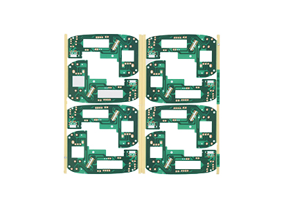


Compact electronic products are becoming smaller, faster, and more function-rich. Therefore, the pcb circuit board must support dense routing, fine-pitch components, reliable stack-up design, stable signal paths, and practical assembly review from the early project stage.
In compact electronics, the printed board is no longer just a base for components. Instead, it controls routing density, signal behavior, power delivery, heat spreading, mechanical fit, and assembly stability inside a limited outline.
For example, a phone module, wearable sensor, camera board, wireless module, medical device board, or industrial controller may include fine-pitch ICs, connectors, RF sections, memory, power circuits, and test points. As a result, routing space can disappear before the layout is complete.
Therefore, hdi pcb manufacturing becomes useful when compact designs need microvias, blind vias, buried vias, via-in-pad routing, or high-density multilayer pcb structures. However, the final build should always depend on design files, material, layer count, surface finish, quantity, and testing requirements.
Why HDI PCB Is Used in Compact Electronics
First, compact products need more connections without a larger board outline. A small pcb circuit board may carry processors, memory, sensors, RF chips, charging circuits, display connectors, antennas, and power rails. Therefore, routing density becomes a major design limit.
At the same time, fine-pitch components reduce routing channels between pads. Traditional through vias can block inner-layer routing and consume valuable copper area. By contrast, microvias and blind vias can connect selected layers while leaving other layers available for routing.
Moreover, shorter interconnect paths can support better signal planning. High-speed nets still need controlled impedance, clean return paths, and stable reference planes. However, dense via structures make those goals easier to manage in limited space.
In addition, compact products often place heat sources close together. Power management ICs, RF power amplifiers, charging circuits, LED drivers, and motor control sections may create local heat concentration. Therefore, copper area, thermal vias, stack-up balance, and component spacing need early review.
Key reasons for using high-density interconnect design
- More routing channels: Microvias can open routing paths around fine-pitch ICs and compact connector areas.
- Smaller board outline: Dense routing can reduce area pressure without removing important functions.
- Selective layer connection: Blind and buried vias connect target layers without passing through the full board stack.
- Better BGA escape routing: High pin-count ICs become easier to route when through vias do not block every layer.
- Cleaner stack-up planning: Signal, ground, power, and impedance layers can be arranged with fewer compromises.
- Stronger miniaturization support: Smaller modules, thinner devices, and lighter electronic assemblies become more practical.
However, higher density also increases manufacturing sensitivity. Microvia diameter, pad size, annular ring, copper thickness, lamination sequence, resin filling, and registration tolerance all affect feasibility.
For this reason, compact board design should not be judged only by the layout image. The practical question is whether the trace width, spacing, via structure, solder mask clearance, copper balance, and assembly process match real production limits.
Consumer and Communication Devices
Consumer electronics often combine many functions in one small product. Smartphones, tablets, wearable devices, wireless audio products, smart home controllers, camera modules, and handheld terminals all need compact and stable board layouts.
For example, a smartphone mainboard may include an application processor, memory, RF transceiver, power management, display connector, camera interface, charging section, and sensor circuits. Therefore, the board must route many signal types without creating unnecessary noise or interference.
Similarly, wearable devices create strict mechanical limits. Smart watches, health bands, GPS trackers, and compact medical wearables may need a thin board, a small battery, wireless communication, sensor inputs, charging contacts, and compact connectors.
Meanwhile, communication modules add RF and high-speed challenges. Wi-Fi, Bluetooth, GNSS, IoT, 4G, and 5G-related boards may need antenna clearance, shielding, controlled impedance, and stable grounding. Therefore, layout review should include both electrical and mechanical constraints.
Common compact product applications
- Smartphones, tablets, handheld terminals, and compact computing products.
- Smart watches, activity trackers, GPS bands, and wearable health devices.
- Bluetooth earbuds, wireless audio boards, microphone modules, and charging cases.
- Camera modules, image sensor boards, video transmission boards, and display interface boards.
- Wi-Fi modules, Bluetooth modules, GNSS boards, IoT gateways, and smart home controllers.
- Portable test instruments, barcode scanners, field meters, and compact payment terminals.
Moreover, high-speed digital interfaces need stable reference planes. MIPI, USB, PCIe, Ethernet, LVDS, and memory interfaces may require controlled impedance and length planning. A dense board can help routing, but the stack-up still controls much of the final electrical result.
Finally, antenna placement should be reviewed with the enclosure. Copper pours, ground vias, shielding cans, batteries, metal parts, and connectors can affect RF areas. Therefore, mechanical drawings and RF layout notes should be checked together.
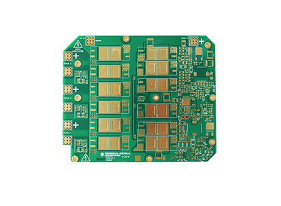
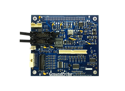
HDI Board Examples for Compact Electronic Projects
The following PCBXINSHUN product images are suitable references for compact boards with dense routing, fine component areas, multilayer structures, and panelized small-board production. Each image and button links to the related HDI Board product category page.

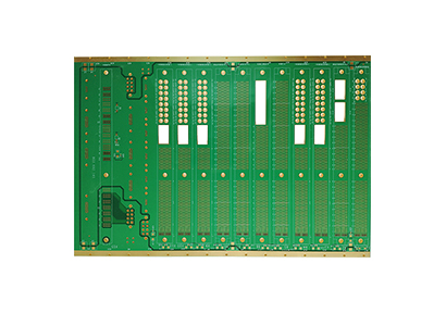
Dense Routing Board
Suitable for compact layouts with fine-pitch pads, multiple routing zones, connectors, and dense signal paths.

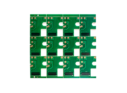
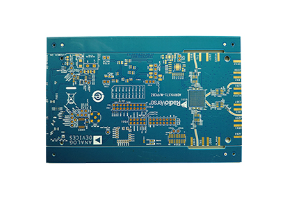
Panelized Compact Boards
Useful for projects that need panel format review, tooling rails, inspection access, and repeated small-board assembly.

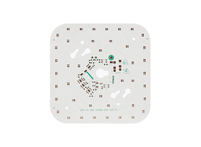
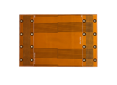
Small Module Panel
Helpful for compact modules that require consistent panelization, pad control, and assembly-oriented board planning.
Medical and Automotive Electronics
Medical electronics often require compact boards with stable sensing, low noise, and careful assembly control. Portable monitors, wearable sensors, diagnostic modules, hearing devices, compact test accessories, and handheld instruments may combine analog inputs, digital control, wireless communication, and battery circuits.
In these products, layout discipline is important. Low-level sensor signals should stay away from switching regulators, clock lines, and RF sections. Therefore, grounding, shielding, component placement, and stack-up design should support signal stability.
Automotive electronics create another set of design pressures. Camera modules, radar boards, lighting controllers, battery management submodules, keyless entry boards, infotainment boards, and compact motor controls must often fit inside restricted housings.
At the same time, vehicle modules may face vibration, heat, connector stress, and electrical noise. Therefore, mechanical support, copper design, thermal relief, connector placement, and inspection planning should be reviewed before layout release.
Medical electronics review points
- Sensor signal routing, analog separation, and grounding approach.
- Wireless section location, antenna keep-out areas, and RF notes.
- Battery charging circuits, protection devices, and thermal behavior.
- Connector orientation, enclosure fit, component height, and assembly direction.
- Testing access, programming pads, inspection requirements, and revision control.
Automotive electronics review points
- Operating environment, including heat, vibration, and connector stress.
- High-speed routing, controlled impedance, and reference plane continuity.
- Power input protection, grounding, shielding, and noise control.
- Thermal concentration around regulators, driver circuits, LEDs, and power ICs.
- Mechanical outline, mounting holes, keep-out areas, and housing tolerance.
Meanwhile, documentation must stay consistent. Gerber files, drill files, stack-up data, fabrication drawings, BOM, placement files, and assembly drawings should refer to the same revision.
Also, a previous standard multilayer pcb design may not transfer directly into a smaller high-density version. Smaller space changes via selection, copper balance, routing direction, component spacing, and assembly risk.
Industrial Control Applications
Industrial control products are not always pocket-sized. However, many modern control modules now need more functions inside smaller cabinets, plug-in cards, sensor housings, and automation devices.
As a result, dense boards appear in PLC modules, motor control boards, robotics controllers, sensor interface boards, compact power modules, data acquisition boards, industrial gateways, and communication adapters.
Industrial boards often mix logic control, power conversion, isolation, connectors, analog measurement, and communication ports. Therefore, layout work must manage spacing, heat, current flow, signal integrity, and inspection access at the same time.
For example, a compact motor control board may include MCU control, gate drivers, current sensing, voltage sensing, communication interface, connectors, and protection devices. If board space is limited, routing channels can disappear quickly.
Where dense board structures help industrial products
- Compact PLC input and output modules with dense connector zones.
- Servo drive control boards with processors, gate drivers, and sensing circuits.
- Robotics controller boards with motion control and feedback signals.
- Smart sensor boards with analog front ends and digital processing.
- Industrial gateway boards with Ethernet, wireless, and serial communication ports.
- Compact power management boards with monitoring and protection circuits.
However, density should not reduce required spacing. Industrial electronics may carry higher voltages, stronger noise, or larger current paths. Therefore, creepage, clearance, copper width, isolation gaps, and thermal relief should remain visible in the review.
In addition, serviceability matters. Programming pads, test points, connector labels, and inspection zones help production and troubleshooting. A compact layout should still leave practical access for testing and repair analysis.
Which Projects Are Better Suited for HDI Board Manufacturing?
Not every compact board requires an advanced interconnect structure. Therefore, the decision should start with routing pressure, component pitch, mechanical size, signal speed, power density, and assembly requirements.
A simple control board, low-speed indicator board, or large connector board may work well with a standard structure. However, a compact design with fine-pitch ICs, short signal paths, and tight board space may need more routing freedom.
| Project Situation | Better Direction | Reason to Review |
| Fine-pitch BGA, CSP, or dense IC package | Consider HDI board structure | Microvias can improve escape routing and reduce blocked channels. |
| Small wearable, camera, RF, or sensor module | Review dense interconnect options | Mechanical limits and component density often create routing pressure. |
| High-speed interfaces or RF transmission | Review stack-up and material carefully | Impedance, reference planes, and signal loss may control performance. |
| Simple low-density board with enough space | Standard multilayer pcb may be enough | Advanced vias may not add value if routing is already simple. |
| Power-heavy board with wide copper needs | Review copper thickness and thermal paths first | Density must not weaken current capacity, spacing, or heat spreading. |
In practical terms, suitable projects often include compact communication modules, mobile device boards, wearable devices, medical sensor boards, automotive camera or control boards, and industrial gateway modules.
By contrast, projects with simple circuits, generous board area, low-speed routing, and no fine-pitch components may not need this manufacturing route. The best decision comes from engineering file review, not from the product name alone.
How Application Requirements Influence Board Structure
Different applications create different board requirements. Therefore, a wearable sensor, a phone module, an RF board, a vehicle camera, and an industrial controller should not use the same design assumptions.
First, component pitch affects routing. Fine-pitch BGAs, CSP packages, small connectors, and dense passive arrays may need microvia escape routing. Without it, the design may require more layers or a larger board outline.
Second, signal speed affects stack-up planning. High-speed interfaces need reference planes, controlled impedance, short return paths, and careful differential pair routing. If the stack-up is weak, later layout changes may not solve the core issue.
Third, power density affects copper design and heat control. Charging circuits, regulators, motor drivers, LED drivers, and RF power sections can concentrate heat in very small areas.
Finally, mechanical design affects everything. Board outline, slots, mounting holes, stiffeners, shielding cans, display position, battery space, and connector direction can change routing strategy and panelization.
| Application Area | Typical Design Pressure | Review Focus |
| Phone and wearable boards | Small outline, thin stack-up, fine-pitch ICs | Microvias, via-in-pad, surface finish, component spacing |
| Communication modules | RF routing, antenna zones, shielding, high-speed links | Material choice, impedance control, ground vias, stack-up |
| Medical electronics | Low-noise sensing, compact housing, wireless functions | Grounding, analog separation, test access, assembly quality |
| Automotive modules | Vibration, heat, connector stress, signal stability | Copper design, mechanical fit, thermal paths, inspection |
| Industrial control boards | Power, isolation, connectors, communication ports | Spacing, copper thickness, test points, heat management |
Manufacturing and Assembly Factors That Affect Compact Boards
High-density boards can solve space problems, but they also increase process sensitivity. Therefore, layer count, material, copper thickness, via design, solder mask, surface finish, panelization, and testing access should be reviewed before production.
Layer count is often the first factor. More layers can provide routing space and stable reference planes. However, a higher layer count also requires stronger stack-up control and clearer documentation.
Material selection also matters. Standard FR-4 may fit many electronic products, while high-speed or RF boards may need closer laminate review. The correct choice depends on frequency, signal loss target, thermal behavior, thickness, and cost planning.
Copper thickness should match both electrical load and layout density. Thicker copper may help current paths and heat spreading. However, it can make fine spacing and fine etching more difficult.
Surface finish affects solderability and pad flatness. Fine-pitch ICs, BGAs, and small passive components may need a flat soldering surface. Still, the suitable finish depends on component type, storage, assembly method, and project requirements.
For general design reference, IPC standards information includes HDI and microvia-related design resources for printed board structures. This external reference is useful for understanding industry terminology, while actual production decisions still require project file review.
Finally, test access must be planned early. Dense boards can lose test points during layout compression. However, removing too many test points can make electrical testing, programming, and troubleshooting harder.
Key review topics before fabrication
- Minimum trace width and spacing for each copper layer.
- Microvia diameter, laser drill size, pad size, and annular ring.
- Blind via and buried via layer pairs.
- Stacked or staggered microvia structure.
- Controlled impedance values and reference layer selection.
- Board thickness, layer count, material family, and copper weight.
- Surface finish, solder mask clearance, and fine-pitch pad design.
- Panelization method, tooling holes, fiducials, and assembly support.
Design Data Project Teams Should Prepare
Before quotation and engineering review, complete data makes the process clearer. Moreover, it reduces assumptions about layer count, material, copper thickness, surface finish, assembly scope, and testing needs.
Gerber files remain important, but they rarely explain the whole project. Therefore, a useful file package should also include drill data, fabrication drawings, stack-up notes, BOM, placement data, assembly drawings, and inspection instructions.
First, the fabrication drawing should define board thickness, layer count, material request, copper weight, surface finish, solder mask color, silkscreen color, outline tolerance, and special process notes. If controlled impedance is required, the target values and layers should also be listed.
Second, via requirements should be clear. Blind vias, buried vias, microvias, via-in-pad, resin plug holes, copper-filled vias, tented vias, and open vias affect both fabrication and assembly. Ambiguous via notes can create repeated questions.
Third, assembly files should match the board revision. BOM, pick-and-place data, polarity notes, assembly drawings, connector direction, programming method, and functional test instructions should all refer to the same project version.
Recommended file checklist
- Gerber files with copper, solder mask, silkscreen, paste, drill, and outline layers.
- NC drill files with clear plated and non-plated hole information.
- Fabrication drawing with layer count, board thickness, copper weight, material, finish, and tolerances.
- Stack-up drawing with dielectric thickness, copper layers, reference planes, and impedance notes.
- BOM with reference designators, part numbers, package types, quantities, and approved alternatives.
- Pick-and-place file for SMT assembly review.
- Assembly drawing with polarity, connector direction, special components, and inspection notes.
- Testing requirements, including electrical test, impedance test, programming, functional test, or other checks.
Additionally, the intended application should be explained in simple technical terms. A communication module may need RF and impedance review. A medical sensor may need low-noise layout attention. An industrial board may need spacing, connector, and thermal review.
In short, the design package should connect board files with real operating conditions. This helps the manufacturer review feasibility based on project requirements rather than assumptions.
When to Choose PCBXINSHUN HDI Board Manufacturing
A high-density board path makes sense when compact size, fine-pitch components, signal routing, and layer connection planning become difficult with standard through-hole structures. However, the final decision should follow the actual Gerber files and engineering requirements.
For PCBXINSHUN project review, the most useful starting point is a complete file package. Gerber files, BOM, layer count, material, surface finish, quantity, and testing requirements allow the review to focus on manufacturability, assembly feasibility, and suitable process planning.
View PCBXINSHUN HDI BoardFAQ
What products use HDI boards?
Common applications include smartphones, wearable devices, wireless modules, camera boards, medical sensors, automotive control modules, industrial gateways, compact instruments, and smart hardware. However, the final board structure depends on component pitch, signal speed, layer count, material, board outline, and assembly requirements.
Why are HDI boards useful for compact electronic devices?
They help route more connections inside a smaller outline. In addition, microvias, blind vias, buried vias, and via-in-pad structures can create routing channels around fine-pitch components. Therefore, compact products can keep more functions without simply enlarging the board.
Are HDI boards suitable for high-density circuit designs?
Yes, they are often suitable when fine-pitch ICs, compact connectors, short signal paths, and limited board space create routing pressure. Nevertheless, suitability should be confirmed through Gerber files, drill data, stack-up notes, material requirements, and assembly information.
What files are needed before quotation?
Gerber files, NC drill files, fabrication drawing, stack-up, BOM, pick-and-place file, assembly drawing, material request, layer count, surface finish, quantity, and testing requirements should be prepared. If controlled impedance is required, target values and related layers should also be included.
Which factors affect manufacturing or assembly difficulty?
Important factors include layer count, material, copper thickness, trace width, spacing, via diameter, via filling, surface finish, solder mask clearance, component pitch, test access, and panelization. In addition, dense layouts may require closer review for soldering, inspection, and functional testing.
Summary and Practical Procurement Suggestions
Compact electronic products need more than a small board size. They need clear routing, stable stack-up design, practical assembly planning, thermal control, and test access. Therefore, early file review can reduce redesign risk and make manufacturing discussion more accurate.
In communication, medical, automotive, and industrial control projects, the correct board structure depends on application requirements. Material, layer count, via structure, copper thickness, surface finish, and inspection method should follow the design files rather than a fixed template.
- First, prepare complete data: Gerber, drill, stack-up, fabrication drawing, BOM, placement file, assembly notes, and revision information should match.
- Second, explain the application: Communication, medical, automotive, industrial, wearable, or handheld use can change material, stack-up, spacing, and testing decisions.
- Finally, confirm review requirements early: Layer count, material, surface finish, quantity, controlled impedance, electrical test, functional test, and inspection needs should be stated before production.
Submit Compact PCB Project Files for PCBXINSHUN Review
For compact board manufacturing or assembly review, send Gerber files, BOM, layer count, material, surface finish, quantity, and testing requirements to PCBXINSHUN. In addition, include stack-up notes, controlled impedance requirements, assembly drawings, and functional test instructions when available. These details help evaluate whether hdi pcb manufacturing is suitable for the project.
Contact PCBXINSHUN Back to Top


