
 Shopping Cart
2
Shopping Cart
2


 Smart Quote
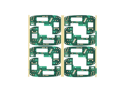


Choosing between a multilayer PCB and an HDI PCB affects routing density, via planning, stack-up design, assembly risk, and manufacturing review. Therefore, the decision should start with circuit density, package pitch, board size, signal requirements, material needs, and testing expectations.
In many electronic products, a standard board with several copper layers can handle routing, power distribution, and ground separation well. However, compact products with fine-pitch BGA, tight SMT placement, short signal paths, and small mechanical outlines may need more advanced interconnect planning.
For industrial controls, communication boards, power modules, LED control boards, and embedded devices, a standard multilayer pcb structure is often a practical starting point. Meanwhile, compact modules and dense digital products may need HDI features because normal through-hole routing can block valuable space.
In other words, the right structure depends on the real layout problem. Layer count, via type, material, copper thickness, surface finish, assembly method, and test scope should support the same project goal.
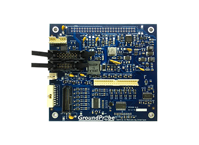
Product Paths for Board Selection
A useful comparison should not stop at definitions. Therefore, the two product paths below connect the selection logic with the next engineering step. Each full image and each button leads to the relevant PCBXINSHUN page.


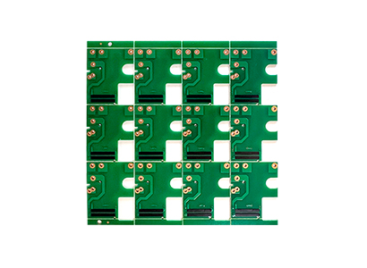
What Is Multilayer PCB?
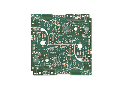
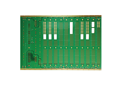
A multilayer printed circuit board contains three or more conductive copper layers. These copper layers are laminated together with insulating materials such as core and prepreg. Therefore, the board can support more complex circuits than a single-sided or double-sided PCB.
Typically, a multilayer stack-up includes signal layers, power planes, and ground planes. The planes help organize power distribution and return paths. As a result, the layout can become cleaner and more stable when the stack-up is planned correctly.
However, a multilayer board does not automatically mean high density. It may still use regular through holes, larger via pads, wider spacing, and conventional routing. Therefore, layer count and routing density should be reviewed separately.
Common Stack-Up Logic
For example, a 4-layer board may use top signal, inner ground, inner power, and bottom signal layers. Meanwhile, a 6-layer or 8-layer board may add more signal layers or reference planes. This allows better routing organization and more flexible circuit separation.
In many industrial and control products, this structure works well because the board outline is not extremely small. In addition, connector areas, power areas, and digital areas can often be separated without advanced via structures.
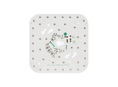
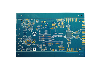
What Is HDI PCB?
HDI means high density interconnect. An hdi pcb uses finer routing, smaller vias, and higher connection density than a conventional board. Therefore, it helps place more electrical connections into a smaller PCB area.
A high density interconnect PCB may use microvias, blind vias, buried vias, via-in-pad, and sequential lamination. Meanwhile, these structures help dense components fan out without sending every via through the full board thickness.
However, HDI is not only a smaller version of a standard board. It requires more careful stack-up planning, drilling control, lamination review, via filling review, surface finish selection, and assembly coordination.
Why HDI Becomes Necessary
HDI becomes useful when standard through-hole routing blocks the layout. For example, the inner rows of a fine-pitch BGA may not escape cleanly with ordinary vias. In that case, microvias or via-in-pad may provide a more practical fanout route.
At the same time, HDI should be selected for a real technical reason. If the board outline is large enough and components have enough spacing, standard multilayer construction may remain the better option.
Structure and Via Differences
The biggest difference is not only the number of layers. Instead, the key difference is how layers connect. A conventional multilayer board often uses plated through holes, while HDI may use microvias, blind vias, buried vias, and via-in-pad structures.
Therefore, two boards with the same layer count may have different manufacturing complexity. A 6-layer standard board and a 6-layer HDI board can require very different drilling, lamination, filling, and inspection review.
| Comparison Item | Standard Multilayer Board | HDI Board |
| Main interconnect method | Plated through holes and standard vias | Microvias, blind vias, buried vias, and via-in-pad |
| Routing density | Moderate to high circuit complexity | Very dense layouts and compact products |
| Typical component pressure | SMD parts, connectors, power sections, control circuits | Fine-pitch BGA, CSP, compact QFN, dense modules |
| Space usage | Through holes occupy space across the full board | Short-span vias save routing space on other layers |
| Engineering review focus | Stack-up, copper, hole size, spacing, finish, testing | Microvia design, lamination sequence, via filling, fine lines, assembly risk |
Through Holes
Through holes are drilled from the top side to the bottom side. After plating, they can connect the required copper layers. Therefore, they remain common in many reliable multilayer designs.
However, through holes consume space through the whole board thickness. Even when a connection only needs two layers, the hole still passes through other layers. As a result, dense routing may become difficult near BGA packages or tight connector groups.
Blind Vias, Buried Vias, and Microvias
Blind vias connect an outer layer to one or more inner layers. Buried vias connect inner layers only. Meanwhile, microvias usually connect short layer spans and support dense fanout.
Consequently, these structures can free routing channels that ordinary through holes would block. Still, the final process depends on project requirements, material selection, layer count, via span, and design files.
Application Differences
Application context often explains the board choice better than a simple definition. A large industrial controller may need several layers for power, ground, and signal routing. However, it may not need microvias if the component spacing is generous.
In contrast, a compact wireless module may need HDI even with fewer total layers. Therefore, board size, package pitch, routing pressure, and assembly method should be reviewed together.
Industrial ControlStandard multilayer construction often fits control boards, I/O modules, relay circuits, and power distribution sections. | Communication ModulesHDI may help when dense BGA, RF modules, compact connectors, or short signal paths create layout pressure. |
Medical and Sensor ElectronicsCompact electronics often need dense routing, stable assembly planning, and careful package-pitch review. | Power ElectronicsWider copper, thermal flow, spacing, and current capacity may matter more than interconnect density. |
Additionally, one product may use both structures across different modules. For example, a power board may use a conventional multilayer structure, while a compact control board may use HDI. This approach can make the full product easier to manufacture and assemble.
However, one board can also combine different functional zones. A power area may need wider copper, while a digital area may need dense fanout. Therefore, the structure should reflect actual circuit zones, not only the product category.
Best Fit: When Each Board Type Makes Sense
A clear selection section helps engineering and sourcing teams move from reading to action. Therefore, the points below translate the technical comparison into practical project fit.
Standard Multilayer Board Is a Better Fit When
| HDI Board Is a Better Fit When
|
How to Choose for a Project
A practical selection process starts with the layout problem. First, check whether the circuit can route cleanly with standard trace width, spacing, pad size, and plated through holes. If routing remains clear, a conventional multilayer structure may be enough.
However, if the layout has fine-pitch BGA, dense SMT placement, a small outline, or blocked escape routing, HDI should be reviewed. In addition, assembly constraints should be checked at the same time because dense PCB problems often become soldering problems later.
1. Check Component Package Density
Component package type is often the first decision point. Fine-pitch BGA, CSP, dense QFN, small connectors, and miniaturized modules can limit routing space. Therefore, pad pitch and fanout strategy should be reviewed before the layer count is locked.
If ordinary vias cannot escape signals without violating spacing rules, microvias may help. Meanwhile, via-in-pad may support compact routing under dense components. However, soldering and via filling requirements should be reviewed before production.
2. Review Board Size and Mechanical Limits
Board outline can force the structure decision. A larger board may allow standard routing even with many circuits. However, a smaller board may need HDI because every via pad and routing channel becomes valuable.
In enclosure-driven products, connectors, mounting holes, keep-out zones, heat sinks, and battery areas reduce usable layout space. Therefore, mechanical drawings should be reviewed early. Otherwise, routing may look possible until the final enclosure restrictions appear.
3. Consider Signal Speed and Impedance
High-speed signals need stable return paths, controlled impedance, and careful layer transitions. Therefore, stack-up planning matters for both board types. The board structure alone does not guarantee signal integrity.
However, HDI can reduce unnecessary stubs and shorten certain routes. This may help dense digital designs when layout, material, and stack-up are planned correctly. At the same time, dielectric thickness, copper thickness, and surface finish can affect final performance.
4. Evaluate Thermal and Current Requirements
Thermal and current requirements can change the best choice. Power circuits, motor control boards, LED drivers, and charging modules may need thicker copper, larger copper pours, thermal vias, and careful spacing.
In some cases, a spacious multilayer layout is more practical than a dense HDI layout. Therefore, routing density and power density should be reviewed separately before the stack-up is finalized.
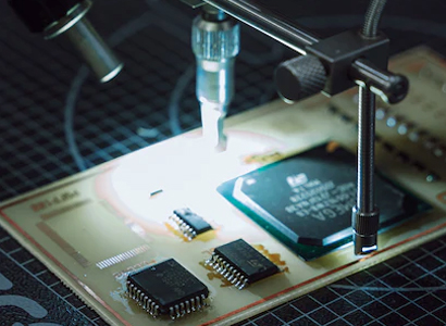
Manufacturing and Assembly Factors
Manufacturing feasibility depends on more than the board name. Trace width, spacing, hole size, annular ring, copper balance, stack-up symmetry, material type, and surface finish all affect the review result. Therefore, fabrication rules should guide the layout from the beginning.
For HDI designs, the review also needs via span, microvia structure, lamination sequence, via filling, and dense pad design. In addition, assembly review should check solder mask openings, paste layer design, component spacing, BGA fanout, polarity marks, and inspection needs.
Key Factors That Affect Fabrication Review
- Layer count: More layers may help routing, but they may not solve fine-pitch fanout problems.
- Material: Electrical, thermal, and mechanical needs should define the material request.
- Copper thickness: Thicker copper can support current, but it may limit fine-line capability.
- Surface finish: Pad flatness, solderability, storage, and component pitch influence the finish choice.
- Testing: Electrical testing, impedance testing, and assembly inspection should match project requirements.
For external design terminology, the IPC-2226 HDI printed board design standard is a useful reference when reviewing high density interconnect structures. However, the final process still depends on the actual production files and manufacturing review.
Meanwhile, incomplete documentation can slow quotation and engineering review. A clean file package allows stack-up, drilling, material, surface finish, and PCBA notes to be reviewed together. As a result, avoidable questions can be reduced before fabrication starts.
Data to Prepare Before Quotation
Good project data helps engineering review move faster. Therefore, the RFQ package should show both PCB fabrication requirements and assembly-related details when PCBA support is needed.
Gerber and Drill FilesCopper, solder mask, silkscreen, paste, outline, hole size, and via structure should match the latest design version. | BOM and Assembly DataPart number, package type, quantity, placement file, polarity note, and special assembly request help PCBA review. |
Stack-Up and MaterialLayer order, copper weight, board thickness, impedance needs, and material request should be clearly listed. | Quantity and TestingPrototype, pilot run, production quantity, electrical test, impedance test, and inspection needs should be included. |
PCB XINSHUN Manufacturing Support
PCB XINSHUN supports PCB and PCBA projects that require structured engineering review before fabrication. Therefore, the focus is not only producing a board from files. It also includes checking whether the selected structure matches the layout, assembly method, and end-use requirements.
For standard multilayer boards, review may focus on layer count, copper thickness, material, solder mask, surface finish, hole size, impedance, and testing needs. Meanwhile, for HDI projects, review may also include microvia structure, via-in-pad, blind and buried via spans, lamination sequence, and fine-pitch assembly concerns.
However, every project remains different. Material, layer count, via structure, surface finish, quantity, and testing requirements all affect manufacturing planning. Therefore, final structure selection should come from real design files rather than a general comparison alone.
View Technical CapabilitiesConclusion: Match the Board Type to the Real Design Problem
The right board structure starts with the design challenge. A standard multilayer board can support many complex electronics when routing space, via size, and assembly layout remain practical. However, HDI becomes important when compact size, fine-pitch packages, and dense routing exceed standard interconnect limits.
Therefore, the decision should consider circuit density, mechanical space, component pitch, signal requirements, thermal needs, material selection, and testing expectations together. For a clear review, PCBXINSHUN can evaluate Gerber files, BOM, layer count, material, surface finish, quantity, and testing requirements before confirming whether multilayer PCB or HDI PCB is the better direction.
- First, review layout density. Check BGA pitch, via space, trace width, spacing, and escape routing before choosing the structure.
- Second, prepare complete files. Submit Gerber files, drill data, BOM, stack-up notes, material, surface finish, quantity, and test requirements.
- Finally, align PCB and PCBA early. Dense boards should be checked for fabrication and assembly at the same time.
FAQ
Prepare Files for PCB XINSHUN Review
For project evaluation, submit Gerber files, BOM, layer count, material request, surface finish, quantity, and testing requirements. In addition, include stack-up notes, impedance targets, blind or buried via details, microvia requirements, and assembly drawings when available.
With complete data, PCBXINSHUN can review whether a standard board, HDI structure, or high density interconnect PCB option fits the design. This review helps align fabrication, PCBA planning, and quotation details before production starts.
Contact PCB XINSHUN


