
 Shopping Cart
2
Shopping Cart
2


 Smart Quote
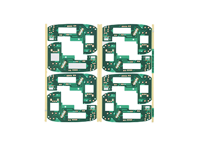


A multilayer PCB helps compact electronics carry more signals, manage power more cleanly, and support stable assembly when a simple PCB board can no longer meet routing, density, or reliability requirements.
Modern electronics depend on more than copper traces. Stable products often need planned layer order, reliable vias, suitable laminate, clean power distribution, controlled return paths, and complete assembly data. The board structure should match the circuit function before fabrication starts.
For project review, PCBXINSHUN’s multilayer PCB product page can help buyers compare layer count, material selection, surface finish, PCB fabrication, PCBA support, and testing requirements before sending a quotation request.
What Is a Multilayer PCB?
A multilayer printed circuit board uses three or more conductive copper layers. These layers connect through plated holes, vias, blind vias, buried vias, or other interconnection structures. The board can route signals, distribute power, and support components inside one compact structure.
In practice, this term can cover four-layer, six-layer, eight-layer, ten-layer, and higher-layer boards. Layer count alone does not define quality. Stack-up design, laminate choice, copper balance, hole design, and manufacturing rules all affect the final result.
A simple PCB board may work well for low-density circuits. Denser products often need internal power and ground planes, shorter routes, and cleaner signal references. Multilayer construction becomes useful when product size, component count, and electrical performance all matter.
Early signs that a design may need more layers
- Dense ICs, fine-pitch packages, BGA devices, or limited routing channels.
- High-speed interfaces, controlled impedance, RF sections, or sensitive analog areas.
- Power planes, ground planes, current distribution, or noise reduction needs.
- Compact mechanical outline, fixed mounting holes, and connector position limits.
How the Structure Works
The structure starts with copper-clad laminate, prepreg, and copper foil. The laminate provides mechanical strength and insulation. Prepreg bonds the layers during lamination. Material choice affects rigidity, thermal behavior, dielectric performance, and long-term stability.
Each copper layer receives a purpose during stack-up planning. Some layers carry signals, while others serve as power or ground reference planes. This helps reduce loop area, improve return paths, and support cleaner voltage delivery.
A good stack-up is not only a layer list. It must consider dielectric thickness, copper weight, target impedance, hole structure, final board thickness, and assembly process. Electrical design and manufacturability need to move together.
Core, prepreg, copper, and vias
A core is a cured laminate with copper on one or both sides. Prepreg is resin-rich glass material that bonds cores and copper foils under heat and pressure. Lamination quality affects layer registration, board thickness, and internal insulation.
Vias create vertical connections between layers. Through holes pass through the full board. Blind vias connect an outer layer to internal layers. Buried vias connect internal layers only. Via type changes routing density, process complexity, and inspection planning.
| Structure item | Why it matters | Review focus |
| Layer count | Defines routing capacity and stack-up direction. | Match density, signal speed, and power needs. |
| Material | Affects thermal, dielectric, and mechanical behavior. | State FR-4 grade or special material needs when required. |
| Copper weight | Influences current capacity, heat rise, and etching tolerance. | Balance current demand with line width and spacing. |
| Via type | Controls vertical connections and routing density. | Confirm drill size, blind vias, buried vias, and via-in-pad notes. |
Benefits for Complex PCB Board Projects
More layers provide more routing channels. A compact PCB board may include processors, memory, sensors, power modules, connectors, displays, and communication interfaces. With internal layers, the layout can avoid long detours and unsafe trace spacing.
Internal power and ground planes improve electrical behavior. A stable ground plane supports cleaner return paths. A planned power plane supports lower impedance distribution. Fast switching loads and mixed-signal areas become easier to manage.
Multilayer construction can also reduce board size. Smaller outlines help products with tight enclosures, fixed mounting points, and connector limits. The compact layout still needs proper spacing, hole tolerance, and assembly clearance.
Signal integrity
Shorter routes, reference planes, and controlled stack-up help high-speed signals remain more stable.
Power stability
Internal planes help current distribution and reduce weak power paths in dense layouts.
Layout density
More layers help route fine-pitch ICs, connectors, and compact modules with fewer compromises.
Suitable Projects and Practical Selection Logic
A strong technical decision should not stop at definitions. This section explains when the structure makes sense and when a simpler board may be enough. It helps engineering and procurement teams prepare better files before sending a quotation request.
In many projects, the right choice depends on density, signal speed, mechanical size, current load, test requirements, and assembly process. Cost control still matters. The goal is not to choose the most complex board, but to choose the structure that matches the product risk.
Best for these projects
- Industrial control boards with power, signal, and communication sections.
- Communication modules, network devices, gateway boards, and RF-related layouts.
- Compact electronics with BGA, QFN, fine-pitch ICs, or dense connectors.
- Medical, test, energy, and automation boards that need stable signal paths.
- PCBA projects where board design, BOM, assembly, and inspection must align.
May not be necessary when
- The circuit is low density and routes cleanly on one or two layers.
- No controlled impedance, high-speed routing, or power plane is required.
- The product has enough board area and simple component placement.
- A quick functional prototype can use a simpler PCB board first.
- The design files are not mature enough for final stack-up confirmation.
Multilayer PCB vs HDI PCB Context
An HDI PCB is usually a high-density interconnect board with finer lines, smaller vias, microvias, and more compact routing structures. HDI may belong to the broader multilayer family, but the two terms are not always the same.
A conventional multilayer board may use standard through holes and regular routing rules. By contrast, an HDI PCB may use laser-drilled microvias, sequential lamination, via filling, and tighter design rules. HDI fits very compact designs or high-pin-density components.
HDI should solve a real problem. If normal trace width, spacing, via size, and layer count can route the circuit safely, a conventional structure may be more practical. The decision should depend on component pitch, board outline, routing density, and reliability requirements.
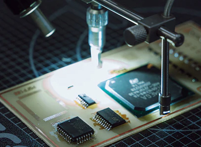
Manufacturing and Inspection Points
Manufacturing review begins with complete design data. Gerber files, drill files, stack-up notes, impedance requirements, material requirements, solder mask, silkscreen, surface finish, and quantity all shape the review. Missing information can delay confirmation.
Layer count affects lamination control, registration tolerance, drilling, plating, routing, and inspection planning. As the structure becomes more complex, small layout problems can create hidden risk. DFM review should happen before production release.
Assembly requirements can also change board design. Via-in-pad, fine-pitch pads, BGA breakout, connector hole tolerance, thermal relief, and test point access all affect PCBA stability. Fabrication and assembly data should be reviewed together when components will be mounted.
Key factors that affect fabrication or assembly
- Layer count: affects lamination, stack-up design, drilling, and registration allowance.
- Board thickness: affects connectors, mechanical fit, aspect ratio, and handling.
- Copper weight: affects current capacity, etching precision, spacing, and heat behavior.
- Minimum trace and spacing: affects manufacturability around fine-pitch components.
- Surface finish: affects solderability, pad flatness, storage, and assembly compatibility.
- Testing needs: may include electrical test, impedance test, inspection notes, or project-specific checks.
Industry reference
For broader PCB design, fabrication, assembly, and inspection terminology, IPC standards are widely used across electronics manufacturing as an industry reference for quality, reliability, consistency, and communication between designers and manufacturers.
How to Prepare Project Data Before Quotation
Gerber and drill files should show the final copper, solder mask, silkscreen, paste, hole, and outline data. File names should match the revision, so the engineering review can avoid confusion between old and new designs.
Stack-up information should define layer order, copper weight, dielectric assumptions, final thickness, and controlled impedance targets when needed. The board can then be reviewed against both electrical and manufacturing requirements.
A BOM becomes essential when PCBA is included. The BOM should list reference designators, quantity, manufacturer part number, package, description, and approved alternatives. Assembly drawings and centroid data help confirm component placement.
Recommended file package
- Gerber files and drill files.
- Stack-up drawing, layer count, board thickness, and material notes.
- Copper weight, surface finish, solder mask, silkscreen, and tolerance requirements.
- BOM, centroid data, assembly drawing, polarity notes, and approved alternatives for PCBA.
- Quantity, testing requirements, packaging needs, and project revision information.
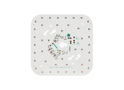
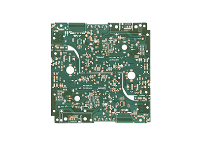
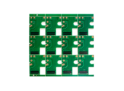
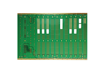
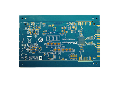
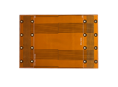
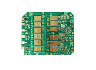
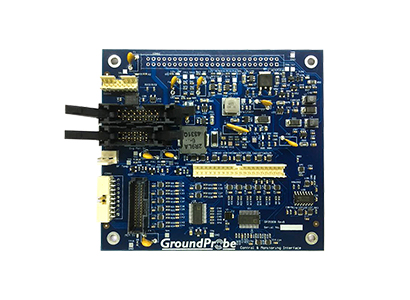
Related PCBXINSHUN Product Directions
The following product directions connect technical reading with practical PCBXINSHUN product pages. Each image is clickable and opens the matching product page. The buttons below the images give a clear next step without interrupting the technical flow.


Practical Purchasing and Engineering Advice
A strong procurement decision starts with engineering clarity. The quotation package should explain the product function, target layer count, material preference, assembly scope, and testing needs. This reduces avoidable back-and-forth during review.
The lowest layer count is not always the best choice. Too few layers may create routing congestion, weak return paths, poor power distribution, and difficult assembly. Too many layers may add process complexity without real value.
The practical goal is balance. Confirm whether the circuit can route cleanly, check signal and power requirements, then review assembly constraints, component pitch, hole design, and test strategy before releasing final files.
FAQ
What is a multilayer PCB?
It is a printed circuit board with three or more copper layers. These layers connect through vias and form one laminated structure, so the board can support more routing, cleaner power distribution, and better signal control than many simple two-layer boards.
When should engineers choose a multilayer board?
A multilayer board becomes practical when component density, routing space, high-speed signals, power planes, ground planes, or compact product size make a two-layer structure difficult. It also helps when controlled impedance or cleaner return paths are required.
Is HDI PCB always the same as multilayer PCB?
No. An HDI PCB usually uses finer lines, smaller vias, microvias, and higher interconnection density. A standard multilayer board may use regular through holes and conventional design rules without HDI structures.
Which files are needed for manufacturing review?
Gerber files, drill files, stack-up notes, material requirements, surface finish, layer count, board thickness, quantity, and testing requirements are important for bare board review. For PCBA, BOM, centroid data, assembly drawings, and polarity notes should also be included.
What factors affect fabrication or assembly difficulty?
Layer count, material, copper weight, board thickness, minimum trace and spacing, via structure, impedance needs, surface finish, component package, and testing scope all influence review. Final planning should depend on the actual design files and project requirements.
Summary and Actionable Suggestions
In summary, multilayer construction supports compact electronics, dense routing, stable power distribution, and cleaner signal paths. The correct structure depends on design files, layer count, material, impedance needs, copper weight, assembly scope, and testing expectations.
- Prepare complete Gerber files, drill files, stack-up notes, and fabrication drawings before quotation review.
- Align layer count, material, copper weight, surface finish, and impedance requirements with the real product environment.
- Include BOM, quantity, assembly scope, and testing requirements when PCBA support is part of the project.
Request a PCBXINSHUN Manufacturing Review
For project review, submit Gerber files, BOM, layer count, material, surface finish, quantity, and testing requirements. With complete data, PCBXINSHUN can review the multilayer PCB structure, manufacturing route, assembly needs, and inspection requirements more accurately.


