
Time:2026-06-20 Views:
A reliable pcb board starts long before copper is etched or components are assembled. The real manufacturing process begins with design file review, material selection, stack-up planning, drilling rules, plating control, surface finish choice, and inspection planning. Therefore, a clear production package helps reduce engineering questions, avoid unnecessary revisions, and support a smoother path from Gerber files to finished boards.
This guide explains how the manufacturing flow works and what technical details matter before production. It is written for engineering, sourcing, and project teams that need practical knowledge before submitting a circuit project for quotation, fabrication, or PCBA review.
Article Navigation

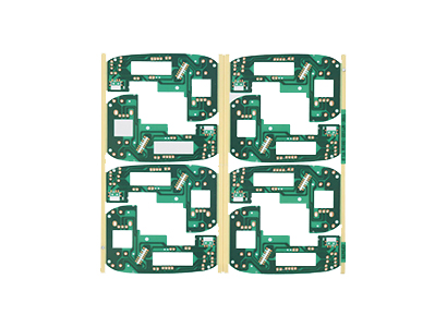
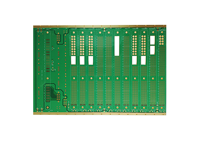
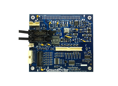
Multilayer, HDI, rigid-flex, thick copper, and assembly-related board categories can be reviewed from the PCB XINSHUN product page. The image and button both lead to the product category page.
View PCB ProductsFirst, design file review checks whether the supplied production data can move into manufacturing without hidden risk. Gerber files define copper layers, solder mask, silkscreen, paste openings, drill information, and board outlines. However, the file package also needs enough context to explain the intended manufacturing result.
In practice, Gerber files act as the production language for a pcb circuit board. They convert layout data into process instructions used during CAM review and fabrication preparation. Therefore, missing drill files, unclear layer names, mismatched board outlines, or outdated revisions can delay production review.
Moreover, a fabrication drawing adds details that Gerber files may not fully explain. It should show board size, thickness, copper weight, material preference, surface finish, solder mask color, silkscreen color, controlled dimensions, and special mechanical requirements. As a result, the manufacturing team can review the project against measurable data instead of assumptions.
Meanwhile, drill files deserve careful attention. They define plated holes, non-plated holes, slots, vias, mounting holes, and finished hole sizes. If a drawing does not separate plated and non-plated features clearly, the wrong process path may be selected. Therefore, hole tables should show quantity, diameter, tolerance, plating requirement, and special slot notes where needed.
A clear file package reduces back-and-forth review. It also helps quotation, engineering review, fabrication planning, and assembly preparation stay aligned. Therefore, every submitted version should be organized with a visible revision number.
Additionally, the BOM should be complete when assembly is included. It should list reference designators, quantities, values, footprints, manufacturer part numbers, and approved alternatives. This prevents sourcing confusion and helps assembly planning start from accurate component data.
For reference, IPC electronics manufacturing standards are widely used across design, fabrication, assembly, inspection, and quality communication in the electronics industry. Therefore, technical drawings and acceptance requirements should be written clearly enough to support consistent review. A useful external reference is the official IPC standards page.
Next, material selection affects electrical behavior, heat resistance, soldering performance, mechanical strength, and long-term reliability. FR-4 is common for many standard electronics projects. However, FR-4 materials can differ in glass transition temperature, dielectric behavior, resin system, copper foil type, and thermal performance.
Therefore, material choice should follow real operating conditions. A low-power control circuit may need standard laminate and normal copper thickness. By contrast, a power board, communication module, LED board, or high-speed circuit may require closer review of temperature, current, impedance, and dielectric stability.
In addition, copper weight should match routing and current needs. Heavier copper can support stronger current paths, but it also affects etching control and spacing rules. Meanwhile, thinner copper may support finer signal routing but may not fit high-current requirements without wider traces.
Board thickness also influences mechanical fit and production behavior. A thin board can suit compact products, yet it may bend more easily during thermal processing. A thicker board may improve rigidity, but it can affect finished hole plating and connector engagement. Therefore, board thickness should be reviewed together with enclosure design, connector requirements, and layer count.
Material review points before production
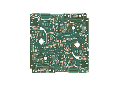
A multilayer pcb requires more planning than a simple single-sided or double-sided board. The stack-up may include cores, prepregs, copper foil, internal signal layers, power planes, and ground planes. During lamination, heat and pressure bond these layers into one stable board structure.
However, internal layers cannot be repaired after lamination. Therefore, inner layer imaging, inspection, cleanliness, registration, and copper balance all matter before pressing starts. Small issues inside the stack may affect impedance, via connection, insulation, or long-term reliability.
Moreover, controlled impedance depends on the whole stack-up, not only trace width. Dielectric thickness, copper thickness, material properties, reference plane distance, and solder mask can all influence signal behavior. As a result, impedance targets should be stated early with layer location and tolerance expectations.
Copper balance also affects board flatness. Large plane areas on one side and sparse copper on another side can increase warpage risk. Therefore, dense multilayer designs should be reviewed for copper distribution before final release.
Multilayer construction often supports compact layouts, more controlled signal routing, better power distribution, and improved reference planes. It is useful when component density increases or when signal integrity becomes important. However, extra layers should solve a real routing, electrical, or mechanical problem.
For example, industrial control boards may need stable power and signal separation. Communication boards may need controlled impedance and clean reference layers. Power-related circuits may need thicker copper and thermal review. Therefore, layer count should match product function, not only layout convenience.

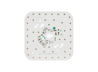
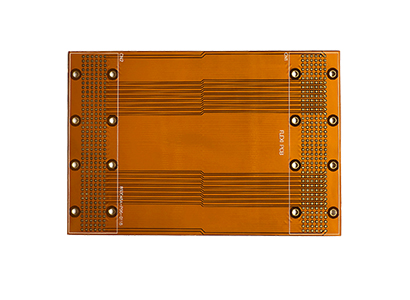
HDI and multilayer board structures are often reviewed when layout density, blind vias, back drilling, or compact signal routing becomes important.
View HDI Board ProductsAfter material and stack-up review, imaging transfers the circuit pattern onto copper. The process uses photoresist, exposure, and development to define which copper areas should remain. Therefore, stable imaging helps maintain trace width, spacing, and pattern accuracy.
Then, etching removes unwanted copper from the panel. Etching control becomes more demanding when copper is heavy or spacing is tight. Consequently, fine traces, small gaps, large copper pours, and thick copper areas should be checked during design review.
Drilling creates vias, through holes, mounting holes, slots, and mechanical features. Mechanical drilling must control tool condition, registration, feed rate, and hole wall quality. In addition, via size and board thickness should be reviewed together because they affect plating stability.
Meanwhile, the annular ring gives tolerance around drilled holes. If the copper pad around a hole is too small, normal drilling movement may reduce connection strength. Therefore, pad size, drill tolerance, finished hole size, and via function should be checked before manufacturing release.
| Factor | Why it matters | Information to prepare |
| Trace width and spacing | They affect etching control, insulation clearance, and yield stability. | Copper weight, voltage needs, and design rules. |
| Finished hole size | It affects drilling, plating, component fit, and solder filling. | Hole table, tolerance, and plated or non-plated status. |
| Board thickness | It affects aspect ratio, stiffness, and connector fit. | Target thickness and tolerance notes. |
| Copper distribution | It influences etching balance, lamination, and warpage risk. | Layer data, plane areas, and stack-up notes. |
Furthermore, slots and cutouts should be marked clearly. A plated slot and a non-plated slot follow different process paths. Therefore, mechanical drawings should identify slot size, tolerance, position, and plating requirement.
Next, plating builds conductive copper inside drilled holes and across selected surfaces. Through-hole plating connects layers electrically and supports component soldering. Therefore, hole preparation, cleaning, activation, copper deposition, and thickness control all influence finished board reliability.
In a common process, electroless copper creates an initial conductive layer on the hole wall. After that, electrolytic copper increases thickness. As a result, drilled holes become electrical paths instead of only mechanical openings.
Surface finish then protects exposed copper and prepares pads for soldering. Common choices may include HASL, lead-free HASL, ENIG, immersion silver, immersion tin, OSP, or other project-specific finishes. However, the correct finish depends on component package, pad flatness, storage time, soldering method, and reliability expectations.
For example, fine-pitch ICs and BGA packages often benefit from flatter pad surfaces. Through-hole or less dense designs may use different finishes depending on soldering needs. Therefore, finish selection should follow assembly requirements rather than appearance alone.
Additionally, solder mask controls solder flow and protects copper traces. Tight solder mask bridges between fine-pitch pads require careful review. If the bridge is too narrow for stable production, mask openings may need adjustment during engineering review.
Silkscreen also supports assembly and repair. It can mark reference designators, polarity, connector orientation, revision codes, and warning notes. However, silkscreen should not cover solder pads or exposed copper. Therefore, silkscreen placement should be checked before release.
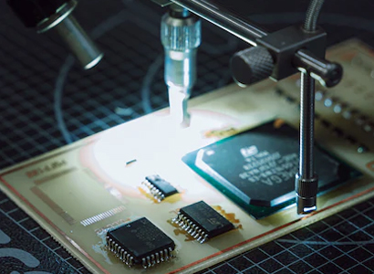
After fabrication, inspection confirms whether the finished circuit matches the intended design. Electrical testing can detect opens, shorts, and connection errors that visual checks may miss. Therefore, netlist data can help compare manufactured connectivity against design intent.
Visual inspection checks solder mask registration, silkscreen clarity, surface finish condition, routing quality, hole quality, and visible defects. However, appearance should be reviewed against agreed acceptance criteria. Vague requirements are harder to inspect consistently.
Dimensional inspection matters when the board fits into an enclosure, connector frame, fixture, or industrial panel. Board outline, slot position, connector edge, mounting hole location, and thickness tolerance can all affect final assembly. Therefore, critical dimensions should be marked clearly on the drawing.
Meanwhile, impedance testing may apply when controlled impedance is required. Stack-up, dielectric spacing, trace width, copper thickness, and material properties all influence results. Consequently, impedance targets and related layers should be stated before production planning begins.
Inspection requirements to define before production
Furthermore, inspection depth should match project risk. A simple LED circuit does not need the same review plan as a dense industrial control board. Still, every design benefits from clean files, clear drawings, and realistic testing requirements.
Fabrication choices directly affect assembly yield. Pad size, solder mask opening, surface finish, board flatness, panel design, and silkscreen clarity all influence SMT and through-hole processing. Therefore, fabrication review and assembly planning should not be separated too late.
For example, solder mask expansion can affect paste control around fine-pitch pads. Too much paste may increase bridging risk, while too little paste may weaken solder joints. As a result, pad geometry should match component package, stencil design, and soldering method.
Thermal balance also affects reflow quality. Large copper areas absorb heat differently from small pads. Therefore, copper distribution, thermal relief design, and component placement should be reviewed before assembly data is finalized.
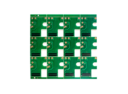
Panelization supports handling during paste printing, placement, reflow, inspection, and depaneling. Rails, fiducials, tooling holes, V-score lines, and breakaway tabs may be required. However, panel design should also reduce mechanical stress during separation.

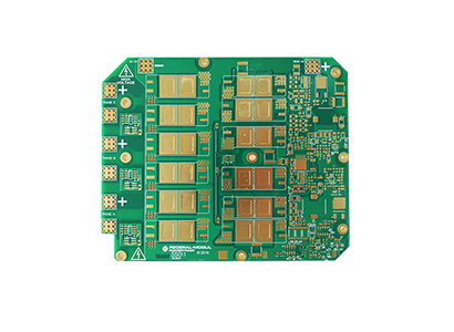
PCBA projects need aligned fabrication files, BOM data, placement files, polarity notes, and inspection requirements. The image and button both lead to the PCB Assembly page.
View PCB Assembly ServiceThis manufacturing flow is useful for projects where design files, material choice, inspection, and assembly readiness matter. It fits early prototypes, small-batch verification, engineering samples, and production preparation. In addition, it supports projects that need stable communication between design, fabrication, and assembly teams.
Industrial control boards often need clear terminal hole sizes, stable copper paths, and reliable soldering areas. Communication boards may require controlled impedance, multilayer stack-up review, and surface finish selection for dense components. Power electronics may need heavier copper, stronger thermal planning, and careful spacing review.
Meanwhile, LED boards, testing equipment boards, medical device control boards, automotive-related electronic modules, consumer electronics, and IoT hardware may all require different review priorities. Therefore, the right production path depends on operating environment, layer count, assembly method, and reliability expectations.
Standard Circuit Projects
Suitable when layout density is moderate and material requirements are straightforward.
Multilayer Electronics
Suitable when routing density, signal separation, power planes, or compact structure matters.
Assembly-Ready Designs
Suitable when BOM, placement, soldering, inspection, and test access need early review.
Before quotation review, the project package should explain what needs to be built and how the finished board will be used. A message with only board size and quantity may not support accurate engineering review. Therefore, the technical package should include design files, manufacturing notes, assembly data, and inspection expectations where relevant.
In addition, special requirements should be stated before production planning. Controlled impedance, tight mechanical tolerance, heavy copper, back drilling, blind vias, buried vias, panelization, special surface finish, and functional testing may affect review scope. However, the correct process depends on project requirements, material, layer count, and design files.
| Submission item | Why it helps |
| Gerber files and drill files | They define the board pattern, holes, outline, and production data. |
| BOM and placement data | They support PCBA quotation, sourcing review, and placement planning. |
| Layer count and stack-up | They help review multilayer structure, impedance, and lamination needs. |
| Material and copper weight | They affect thermal behavior, current capacity, and manufacturing control. |
| Surface finish and quantity | They affect soldering, handling, planning, and quotation review. |
| Testing requirements | They define electrical, dimensional, impedance, or assembly inspection expectations. |
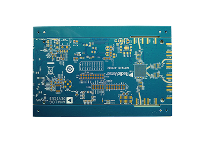
PCB XINSHUN supports circuit projects by reviewing submitted production data and project requirements before manufacturing planning. The review can include Gerber files, drill data, layer count, material notes, copper requirements, surface finish, quantity, and inspection needs. Therefore, the process starts with a complete technical package.
Moreover, different designs require different review priorities. A standard double-sided circuit may focus on material, copper, hole size, solder mask, and surface finish. A multilayer PCB may require deeper review of stack-up, internal layers, impedance, drilling, plating, and lamination. A PCBA project also needs BOM, placement data, soldering requirements, and test access review.
For project teams comparing available categories, multilayer PCB products provide a practical starting point for reviewing board types and related manufacturing directions. This helps connect design needs with the right production category before files are submitted.
However, no accurate manufacturing recommendation can come from a project title alone. Reliable review depends on files, dimensions, layer structure, material preference, finish choice, quantity, and testing scope. Therefore, complete data is the fastest way to reduce assumptions.
Engineering review starts with complete files
Prepare Gerber files, BOM, layer count, material, surface finish, quantity, and testing requirements before requesting project review from PCB XINSHUN.
The following PCB XINSHUN pages can help match this manufacturing process with specific board categories and assembly needs.
PCB Product Categories
Review board categories including multilayer, HDI, rigid-flex, thick copper, and assembly-related options.
Read moreHDI Board
Explore HDI board options for dense layouts, blind vias, back drilling, and compact electronic designs.
Read morePCB Assembly
Review how fabrication files, BOM quality, placement data, and inspection requirements connect with PCBA work.
Read moreA complete package usually includes Gerber files, drill files, a fabrication drawing, material notes, layer count, board thickness, copper weight, surface finish, quantity, and inspection requirements. For PCBA projects, BOM, pick-and-place data, assembly drawings, and polarity notes are also needed.
Gerber files describe copper patterns, solder mask, silkscreen, paste openings, and board outlines. Therefore, they guide the manufacturing process. However, they must match drill files, drawings, and revision notes to avoid production confusion.
Multilayer PCB manufacturing includes inner layer imaging, inspection, lamination, registration control, drilling, plating, and stack-up management. As a result, material selection, dielectric spacing, copper balance, and via design require closer review.
Surface finish selection depends on component package, soldering method, pad flatness, storage time, and inspection needs. Fine-pitch parts and BGA packages often need flatter pads. However, the final finish should follow project requirements.
Clear drawings, complete Gerber files, correct drill data, stable BOM data, and defined inspection requirements reduce uncertainty. In addition, matching revision numbers across all files helps prevent old data from entering production review.
Reliable circuit manufacturing depends on disciplined preparation. Design files, material choice, stack-up planning, imaging, etching, drilling, plating, surface finish, testing, and assembly planning all influence the finished result. Therefore, production review should start with complete and consistent technical data.
In summary, prepare Gerber files, BOM, layer count, material, surface finish, quantity, and testing requirements before submitting a PCB project. This gives PCB XINSHUN enough information to review the pcb board, clarify process needs, and support the next manufacturing step.
Prepare project files for PCB XINSHUN review
For a clearer quotation and engineering review, submit Gerber files, BOM, layer count, material, surface finish, quantity, and testing requirements. Add notes for impedance, tolerance, panelization, assembly, or inspection reports when required.


PCB laminate uses high quality
FR-4 material for PCB production!

3-5days' Delivery
99% on-time shipping

Paypal online guarantees the
instant,convenient, and secure
payment!

Track Fabrication Process On Line
Professional Technical Assistance

PCB XINSHUN fully compliant with the
ISO 9001: quality management
system and UL certificate.
 live:407eab808ea4a40d
 133 1645 5968
 Email:sales@pcbxinshun.com
 Building 2, Wanxia Industrial Zone, No. 32, Xiangxing Road, Baoan District, Shenzhen City, Guangdong Province


 Shopping Cart
2
Shopping Cart
2


 Smart Quote