
Time:2026-06-18 Views:
First, a pcb circuit board turns an electronic design into a real working board. It carries signals, distributes power, supports components, and helps the same product be made again with stable quality. Therefore, understanding board structure, design files, materials, surface finish, and testing needs makes early PCB planning much clearer.
Article Navigation
Moreover, a printed circuit board is not only a flat panel with copper lines. It is a controlled structure made from insulation, copper, drilled holes, plating, solder mask, surface finish, markings, and inspection data. Each part has a job, and each choice can affect production, assembly, and product reliability.
However, early projects often start with only a schematic, a layout screenshot, or an incomplete file set. That is usually not enough for stable pcb manufacturing review. A complete request should connect design intent with Gerber files, BOM data, layer count, material, surface finish, quantity, and testing requirements.
In simple words, a printed circuit board is an insulating base with copper paths on it. These copper paths connect pads, holes, connectors, and component pins according to the circuit design. As a result, the board replaces loose wiring with a cleaner and more repeatable structure.
At the same time, the board gives components a stable place to sit. Components need correct positions for soldering, inspection, and later use. Therefore, board thickness, outline, mounting holes, connector location, and panel format all matter before production.
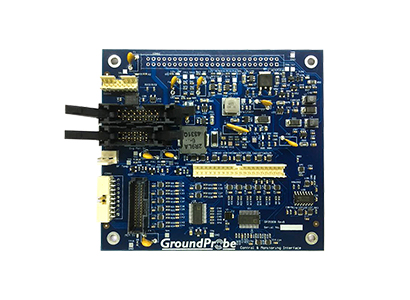
Also, the phrase pcb board often appears in general communication. It usually means the same printed board structure. Still, it is useful to separate a bare PCB from a PCBA, because PCBA means the board already has components assembled on it.
First, the board routes signals. Copper traces move information between chips, sensors, connectors, displays, memory, and power parts. For high-speed designs, trace length, impedance, return path, and layer stack-up need careful review.
Second, the board distributes power. Wider copper areas, power planes, vias, and thermal pads can help current move safely. However, copper thickness and trace width should match the real current load, not a guess.
Third, the board supports heat control. Power devices, LEDs, charging circuits, and motor control sections can create hot areas. Therefore, copper pours, thermal vias, metal-core options, and component placement may affect final performance.
Generally, a bare PCB means the fabricated board before components are mounted. It includes copper layers, drilled holes, plated vias, solder mask, surface finish, and legend markings. However, it does not yet perform the complete electronic function.
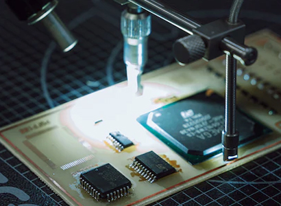
By contrast, PCBA means printed circuit board assembly. This stage adds electronic parts through SMT, through-hole soldering, or a mixed process. In addition, PCBA work may include solder paste printing, pick-and-place, reflow soldering, inspection, programming, and testing.
Therefore, fabrication data and assembly data should be prepared separately. Gerber files support bare board fabrication. Meanwhile, BOM, centroid data, assembly drawings, polarity notes, and test instructions support assembly review.
| Bare PCB | A fabricated board without mounted components. Gerber files, drill files, stack-up notes, and finish requirements guide review. |
| PCB Board | A common general term for a printed board, often used in engineering and sourcing discussions. |
| PCBA | An assembled board with components soldered in place. BOM, centroid data, drawings, and test notes become necessary. |
First, production starts with engineering review. The manufacturer checks Gerber files, drill data, board outline, layer order, material notes, surface finish, copper thickness, and special requirements. Consequently, unclear files can stop review before any panel enters production.
Next, the design data becomes manufacturing data. Panel layout, drill programs, routing paths, electrical test data, and process notes are prepared. Because every board has different spacing, holes, copper areas, and tolerances, this step is important.
Initially, laminate sheets are cut into production panels. The material may be FR-4 or another laminate, depending on electrical, thermal, and mechanical needs. In addition, copper weight should match the current load and layout density.
For multilayer boards, inner layers receive the circuit pattern first. A photo process creates the required copper image, and etching removes unwanted copper. Therefore, hidden inner-layer quality should be checked before lamination.
Moreover, problems at this stage can stay hidden inside the final board. Opens, shorts, scratches, and registration issues should be found early. As a result, inner-layer inspection protects both quality and material use.
After inner layers pass review, cores, prepreg, and copper foil are stacked together. Heat and pressure bond the layers into one solid structure. Therefore, lamination control affects board thickness, insulation, registration, and stability.
Meanwhile, the stack-up is more than the number of layers. It affects impedance, power distribution, noise control, heat behavior, and mechanical balance. For dense or high-speed layouts, stack-up review should happen before final production release.
In addition, copper balance is important. Uneven copper distribution can increase warpage during heat processes. Therefore, plane design, copper pours, and layer symmetry should be considered during layout.
Once the laminated panel is ready, drilling creates holes for vias, component leads, slots, and mounting points. Mechanical drilling is common for through holes. However, special via structures may need additional process review.
Then the drilled holes need conductive copper on the hole walls. Plating builds a copper barrel that connects the required layers. Consequently, plating quality directly affects electrical continuity and long-term reliability.
For example, weak hole plating may pass a simple visual check but fail during heat stress. Rough drilling, resin smear, burrs, and poor copper adhesion can also create risk. Therefore, drilling and plating are key quality-control points.
Next, the outer copper layers receive their final circuit image. This process defines traces, pads, copper areas, and component footprints. After plating and etching, unwanted copper leaves the surface while designed features remain.
However, fine-pitch components and narrow spacing demand tighter process control. Small pads, narrow solder mask bridges, and dense via fields can increase manufacturing risk. Therefore, DFM review should happen before tooling begins.
Also, copper thickness influences etching precision. Heavy copper can support current, but it may reduce fine-line capability. Consequently, high-current and high-density needs must be balanced carefully.
After copper patterning, solder mask protects most exposed copper. The mask helps reduce solder bridges and protects areas that should not receive solder. In addition, mask opening accuracy affects assembly yield around fine pads.
Then legend printing adds reference designators, polarity marks, connector names, and revision information. Although legend is not the circuit itself, it helps assembly, inspection, maintenance, and troubleshooting.
Finally, surface finish protects exposed pads and supports soldering. Options may include HASL, lead-free HASL, ENIG, OSP, immersion silver, or other finishes, depending on project requirements. Therefore, the finish should match component pitch, storage expectations, soldering method, and reliability needs.
After surface finish, routing or scoring creates the final board outline. Slots, cutouts, tooling holes, and panel rails may also be processed. Therefore, mechanical drawings should match enclosure, connector, and fixture requirements.
Next, electrical testing checks for opens and shorts in the bare board network. This does not replace functional testing after assembly. However, it confirms that the fabricated copper connections follow the approved data.
Finally, visual inspection, measurement, packaging, and release checks close the fabrication process. The final standard depends on approved files and agreed project requirements. Therefore, precise documentation matters from the first inquiry.
At the material level, a printed board combines insulating laminate and copper. The laminate provides strength and electrical insulation. Meanwhile, copper creates conductive paths for signals, power, and ground.
However, material choice should not rely on habit alone. A simple control board, LED power board, communication module, industrial controller, or dense HDI board may need different material behavior. Therefore, thermal load, frequency, voltage, size, and assembly method should guide selection.
FR-4 is common in many standard electronics. It offers a practical balance of insulation, strength, and process familiarity. However, FR-4 grades can differ in glass transition temperature, dielectric behavior, and thickness tolerance.
For thermal applications, material selection may focus on heat spreading. LED lighting, power modules, chargers, and motor control designs can create concentrated heat. Therefore, copper area, thermal vias, and possible metal-core options may deserve review.
For high-frequency or high-speed applications, dielectric properties may matter more. Signal loss, impedance control, stack-up stability, and material consistency can affect performance. Consequently, the design package should clearly mention impedance or frequency-related needs.
Copper weight affects current capacity and heat rise. Wider traces and heavier copper can support higher current. However, heavier copper can make fine etching more difficult, especially with dense spacing.
Therefore, copper thickness should match electrical load and layout density. A low-power signal board may not need heavy copper. By contrast, power input paths, motor outputs, LED channels, and battery sections may need more copper area.
In addition, copper balance affects mechanical behavior. Large copper differences between layers can increase warpage. Consequently, layout planning should consider copper pours, plane balance, and panel stability.
Layer count affects routing space, electrical performance, and production complexity. Single-layer and two-layer boards may support simple circuits. However, compact modules and dense IC designs often need four or more layers.
With more layers, power and ground planes can improve return paths and noise control. Also, signal routing can become cleaner. Therefore, layer count should follow real routing, EMC, signal, and thermal needs.
For high-speed designs, the stack-up should not be guessed at the final stage. Dielectric thickness, reference planes, copper weight, and impedance targets should appear in the documentation. As a result, manufacturing review can proceed with fewer assumptions.
Surface finish protects exposed copper before soldering. It also affects pad flatness, storage, solderability, and inspection appearance. Therefore, the selected finish should fit the assembly method and component package types.
For example, fine-pitch ICs and BGA packages may need very flat pad surfaces. Standard components may allow broader finish choices. However, finish selection still depends on project requirements, not a universal ranking.
In addition, storage and handling expectations should be considered. Some finishes need tighter control after production. Consequently, assembly timing and packaging notes should align with the chosen finish.
Before fabrication starts, the design file package should describe the board completely. Gerber files show copper layers, solder mask, legend, paste layers, and mechanical outlines. In addition, drill data defines hole sizes, hole positions, and plated or non-plated status.
However, Gerber files alone may not show every requirement. A drawing or readme file should state units, layer order, material, board thickness, copper thickness, surface finish, quantity, and special notes. Therefore, a structured package reduces avoidable questions.
First, Gerber files define the board image layer by layer. They show traces, pads, copper pours, solder mask openings, legend text, and outline information. Meanwhile, NC drill files define holes and tool sizes.
For multilayer boards, layer order must be clear. A file named inner layer may not explain whether it is a ground plane, power plane, or signal layer. Therefore, a stack-up drawing should be included whenever the board has more than two layers.
Also, plated and non-plated holes should be separated. Vias usually need copper connection between layers. Mounting holes may not need plating. Consequently, hole type clarity prevents wrong assumptions during drilling review.
For assembly, the BOM is essential. It should list reference designators, component values, package types, quantities, manufacturer part numbers, and approved alternatives when available. In addition, it should mark parts that should not be mounted.
Next, centroid data guides SMT placement. It gives component coordinates, rotation, and reference designators. Therefore, it should match the board revision and BOM revision exactly.
Moreover, assembly drawings help confirm polarity and orientation. Diodes, LEDs, ICs, electrolytic capacitors, connectors, and switches can cause errors if markings conflict. As a result, drawing, silkscreen, and component data should tell the same story.
DFM means design for manufacturing. It checks whether the board can be fabricated with stable process control. For example, it may review trace width, spacing, annular ring, hole size, copper-to-edge clearance, solder mask bridge, and panel layout.
DFA means design for assembly. It focuses on placement, soldering, inspection access, component spacing, polarity, and process flow. Therefore, it helps identify issues that may not appear during bare board fabrication review.
In practice, DFM and DFA should happen before tooling release. Small layout changes may improve yield, reduce bridge risk, or improve fixture access. However, all changes should preserve circuit function and mechanical fit.
After the basic board concept is clear, the next step is matching the project to a suitable product path. A simple board, a compact module, a heat-focused power section, and a finished electronic assembly do not need the same route. Therefore, the product category should follow the circuit structure and manufacturing need.
Moreover, this decision should not become a hard product push. The correct path depends on layer count, routing density, current, heat, component package type, inspection method, and final use environment. The table below gives a practical starting point before file review.
At the middle of the research journey, product category pages help connect this guide with practical next steps. PCB XINSHUN provides board-related categories through its PCB product categories page. However, the final choice still depends on actual Gerber files, BOM, layer count, material, finish, quantity, and testing needs.
Therefore, the product cards below are placed as navigation support, not as a forced recommendation. Each image is clickable and leads to the matching product page. The visible button gives the same path for clearer action.
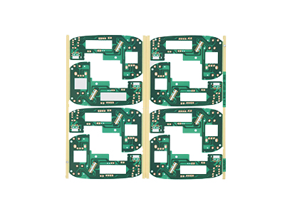
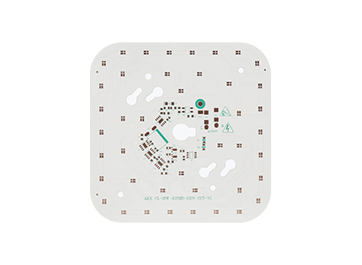
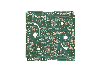
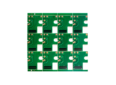
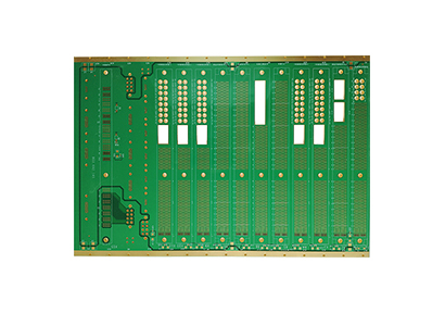
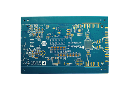
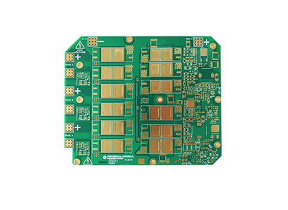
Double Sided PCBMeanwhile, double-sided boards fit standard control circuits, interface boards, and electronic modules that need routing on both sides. Know More | HDI BoardMoreover, HDI boards support compact designs, denser routing, fine-pitch packages, and advanced interconnection needs. Know More | PCB AssemblyIn addition, assembly review connects the bare board, BOM, placement data, soldering process, inspection method, and test plan. Know More |
Several technical factors affect fabrication difficulty and quotation review. Layer count, board size, thickness, copper weight, minimum trace width, spacing, hole size, surface finish, and tolerance all matter. Therefore, board area alone is never enough for a serious production assessment.
In addition, assembly scope can change the full project plan. Fine-pitch ICs, BGAs, through-hole parts, connectors, thermal pads, test points, cables, and coating steps may affect process selection. Consequently, fabrication and assembly should be reviewed together when PCBA is required.
First, layer count affects lamination, drilling, inspection, impedance control, and cost structure. A two-layer board usually follows a simpler route than a multilayer design. However, a small high-density board may still need careful engineering review.
Also, via type affects complexity. Through vias are common, while blind vias, buried vias, microvias, back drilling, or via-in-pad structures need more detailed review. Therefore, the via plan should match the design need and process feasibility.
For compact products, routing density can push limits quickly. Smaller packages, tighter spacing, and many signal nets increase technical pressure. As a result, early stack-up and DFM review can save later redesign time.
Quantity affects material preparation, panel planning, tooling use, inspection flow, and assembly setup. Prototype, pilot, and repeat production stages may need different review depth. Therefore, the requested quantity should match project maturity.
Revision control is equally important. Gerber files, BOM, centroid data, drawings, and test instructions should all share the same revision. Otherwise, an outdated BOM or placement file can create serious assembly problems.
Testing should also be clear. Bare board electrical testing checks opens and shorts. Functional testing needs power conditions, firmware, fixtures, cables, expected outputs, and pass-fail limits. Therefore, the test method should be written before assembly planning.
For engineering reference, IPC standards are widely used in the electronics manufacturing industry to clarify quality, reliability, and production expectations. However, a standards reference should not replace project-specific file review. It works best as background support when discussing PCB design rules, assembly quality, inspection language, and manufacturing consistency.
For electronics manufacturing standards and terminology, review IPC standards information.
PCB XINSHUN is relevant when a project needs board fabrication or assembly review based on complete engineering data. A useful starting point is a file package that includes Gerber files, BOM, layer count, material, surface finish, quantity, and testing needs. Therefore, technical communication can focus on real requirements instead of assumptions.
Moreover, board fabrication and assembly should connect early when PCBA is part of the plan. Bare board choices affect assembly yield, while component data affects soldering and inspection. As a result, fabrication and PCBA planning should not be separated too late.
First, standard control boards can benefit from clear fabrication review. These boards may use common materials and straightforward routing. However, they still need correct files, hole data, finish selection, and testing notes.
Next, dense electronic modules need closer review. Fine-pitch packages, compact connectors, multiple layers, and signal-sensitive sections may require DFM and DFA feedback. Therefore, early communication can prevent avoidable redesign work.
Finally, assembled boards need coordinated review. The BOM, centroid file, polarity notes, fixture access, firmware method, and functional test plan can affect the full path. Consequently, assembly information should be prepared before quotation review.
A practical request should include board purpose, expected operating environment, layer count, material, finish, quantity, and assembly scope. In addition, any controlled impedance, high current, special tolerance, or panel requirement should be highlighted.
For PCBA work, the BOM should include complete component information. If substitutes are acceptable, the BOM should state that clearly. Otherwise, part availability may affect review, quotation, or production planning.
Also, testing requirements should be submitted early. Functional checks may need fixtures, firmware, instructions, and pass-fail criteria. Therefore, testing should be part of the first technical request, not a final-stage add-on.
In addition, these internal pages support the next step after basic learning. They keep navigation focused on real PCBXINSHUN pages and avoid unrelated links.
First, review available PCB board, HDI, rigid-flex, thick copper, and assembly categories.
Open Products PageNext, review solution information for PCB, components, precision manufacturing, and electronics manufacturing.
Open Solutions PageFinally, send files and project requirements through the contact page for practical review.
Open Contact PageOverall, a printed board is the physical foundation of an electronic product. It combines laminate, copper, holes, plating, solder mask, surface finish, markings, and inspection data. Moreover, each technical choice affects manufacturability, assembly yield, and product reliability.
Therefore, project preparation should focus on clarity. The more complete the design files and requirements are, the easier technical review becomes. In addition, clear revision control prevents outdated Gerber files, BOM data, or test notes from entering production.
Finally, submit Gerber files, BOM, layer count, material, surface finish, quantity, and testing requirements for a practical review. Also include notes about controlled impedance, copper thickness, fine-pitch components, panelization, connectors, firmware, fixtures, and functional checks when they apply. With complete data, PCBXINSHUN can review the pcb circuit board specification based on actual project requirements.
Contact PCB XINSHUN View Product Categories Back to Top

PCB laminate uses high quality
FR-4 material for PCB production!

3-5days' Delivery
99% on-time shipping

Paypal online guarantees the
instant,convenient, and secure
payment!

Track Fabrication Process On Line
Professional Technical Assistance

PCB XINSHUN fully compliant with the
ISO 9001: quality management
system and UL certificate.
 live:407eab808ea4a40d
 133 1645 5968
 Email:sales@pcbxinshun.com
 Building 2, Wanxia Industrial Zone, No. 32, Xiangxing Road, Baoan District, Shenzhen City, Guangdong Province


 Shopping Cart
2
Shopping Cart
2


 Smart Quote