| Manufacturing capabilities | Conventional | Unconventional | |||||
|---|---|---|---|---|---|---|---|
| Item | Classify | Project Item | Unit | Prototype | Small Production Volumes | Production Volumes | R&D Capabilities |
| 21 | Product | Finished copper thickness (105um base copper) | um | 140 | 130 | 130 | ≥140 need extra plating |
| 22 | Product | Solder mask colour | Green, Yellow, Black, Blue, Red, White, Matt green, Matt Black | Green, Yellow, Black, Blue, Red, White, Matt green, Matt Black | Green, Yellow, Black, Blue, Red, White, Matt green, Matt Black | Other colour, to be evaluated | |
| 23 | Product | Silk screen colour | White, Yellow, Black | White, Yellow, Black | White, Yellow, Black | Other colour, to be evaluated | |
| 24 | Product | Minimum diameter of BGA pad | mil | 8 | 10 | 12 | ≤8 to be evaluated |
| 25 | Product | Minimum width of etching mark | mil | 6(12,18um), 7(35um), 10(70um) | 8(12,18um), 10(35um), 12(70um) | 8(12,18um),10(35um),12(70um) | |
| 26 | Product | Min Hole-Wall Cu(IPCⅡ, except Blind & Buried Vias) | um | AVG 20, Min18 | AVG 20, Min18 | AVG 20, Min18 | |
| 27 | Product | Min Hole-Wall Cu(IPCⅢ, except Blind & Buried Vias) | um | AVG 25, Min 20 | AVG 25, Min 20 | AVG 25, Min 20 | |
| 28 | Product | Min Hole-Wall Cu(IPCⅡ,Blind & Buried Vias) | um | AVG 20, Min18 | AVG 20, Min18 | AVG 20, Min18 | |
| 29 | Product | Min Hole-Wall Cu(IPCⅢ, Blind & Buried Vias) | um | AVG 25, Min 20 | AVG 25, Min 20 | AVG 25, Min 20 | |
| 30 | Product | Min Hole-Wall Cu(Special requirement) | um | AVG30, Min 25 | AVG30, Min 25 | AVG30, Min 25 | Request AVG≥30um need to evaluated |
| 31 | Product | Nick thickness of Gold Finger | um | >5um | 3-5um | 3-5um | >5um to be evaluated |
| 32 | Product | Gold thickness of Gold Finger | um | 1.0-1.5 | 0.25-1.0 | 0.25-1.0 | >1.0 to be evaluated |
| 33 | Product | Accuracy of solderless hole | mil | ±2 | ±3 | ±3 | |
| 34 | Product | HAL Tin Lead / Tin Min thickness | um | 0.4(Large Tin Surface) | 0.4(Large Tin Surface) | 0.4(Large Tin Surface) | Any requirement need to be evaluated |
| 35 | Product | Maximum diameter for solder mask plug holes | mm | ≥0.65 | 0.6 | 0.5 | ≥0.65 to be evaluated |
| 36 | Product | Minimum width for solder mask opening word | mil | 7 | 8 | 8 | <7mil to be evaluated |
| 37 | Product | Minimum solder mask Thickness | um | Speical requirement | 10 | 8 | Special requirement need to be evaluated |
| 38 | Product | Solder mask thickness of covered vias | um | Speical requirement | 5-8um | 5-8um | Special requirement need to be evaluated |
| 39 | Product | Minimum widith of solder mask bridge | mil | 3.5(green),5(other colour)(Base copper ≤1OZ)(Base copper 2-4OZ, all follows 5mil) | 4(green),6(other colour)(Base copper ≤1OZ)(Base copper 2-4OZ, all follows 6mil) | 4(green),6(other colour)(Base copper ≤1OZ)(Base copper 2-4OZ, all follows 5mil) | Standard <4mil need to be evaluated; Thick copper <6mil need to be evaluated. |
| 40 | Product | Pealable mask thickness | mm | 0.5 | 0.2-0.4 | 0.2-0.4 | ≥0.5 to be evaluated |

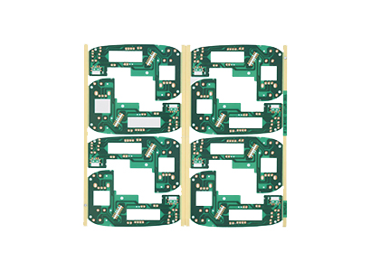
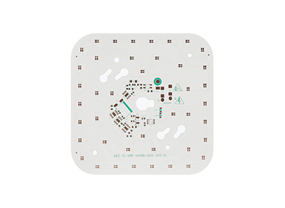
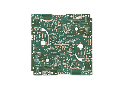
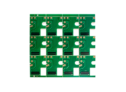
PCB laminate uses high quality
FR-4 material for PCB production!

3-5days' Delivery
99% on-time shipping

Paypal online guarantees the
instant,convenient, and secure
payment!

Track Fabrication Process On Line
Professional Technical Assistance

PCB XINSHUN fully compliant with the
ISO 9001: quality management
system and UL certificate.
 live:407eab808ea4a40d
 133 1645 5968
 Email:sales@pcbxinshun.com
 Building 2, Wanxia Industrial Zone, No. 32, Xiangxing Road, Baoan District, Shenzhen City, Guangdong Province


 Shopping Cart
2
Shopping Cart
2


 Smart Quote