Time:2022-08-26 Views:
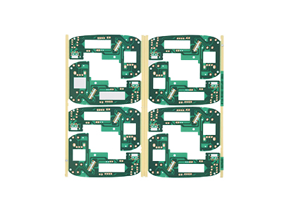
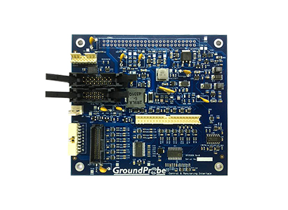
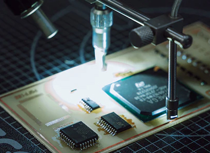
The PCB double-sided circuit board in the smt process workshop adopts the red glue process on one side and the solder paste process of the smt process equipment on the other side. This method is suitable for relatively dense electronic components, and the components on one side are all high and low. Different pcb circuit boards. Especially large electronic components have a large gravity and will fall off after reflow soldering in the smt process workshop. At this time, the red glue will be more firm when heated.
The process flow is: 1. Incoming material inspection 2. PCB A side silk screen solder paste 3. SMD 4. AOI or QC inspection 5. A side reflow soldering 6. Flip board 7. Silk screen red glue or PCB B side dot red glue ( Note that whether it is red glue or silk-screen red glue, the red glue is applied to the middle of the component, do not let the red glue stick to the pad and cause the component feet not to be soldered) > SMD > Dry > Clean > Check > Repair.
Another point to note here is that the solder paste surface must be soldered first, and then the red glue surface should be dried. Because the drying temperature of red glue is relatively low, it can be cured at about 180 degrees. If you dry the red glue surface first, and then operate the solder paste surface, it is easy to cause the electronic components on the pcb circuit board to fall off. When the temperature is as high as more than 200 degrees, it is easy to make the cured red glue fail and become brittle, resulting in a large number of components falling off.
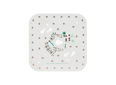
The solder paste process is used on both sides of the pcb circuit board. This method is suitable for IC or BGA pcb boards with a large number of components on both sides and large dense pins on both sides of the pcb board. Because if red glue is dispensed, it is easy to cause misalignment of IC pins and pads.
The process flow is: SMT factory first incoming inspection > PCB's A-side silk-screen solder paste > SMD > QC or AOI inspection > A-side reflow soldering > flip > PCB's B-side silk-screen solder paste > SMD > QC or AOI inspection > reflow soldering > Clean > Check > Rework. Also note here: In order to prevent large components from falling off when passing through the B side of the pcb circuit board, the smt technical operator should set the temperature of the welding area in the lower temperature area of the pad. Reflow soldering is performed while setting the reflow soldering temperature. The temperature of the fusion zone in the upper temperature zone of reflow soldering is slightly lower by 5 degrees. That way, the tin underneath won't melt again and cause the component to come off.


PCB laminate uses high quality
FR-4 material for PCB production!

3-5days' Delivery
99% on-time shipping

Paypal online guarantees the
instant,convenient, and secure
payment!

Track Fabrication Process On Line
Professional Technical Assistance

PCB XINSHUN fully compliant with the
ISO 9001: quality management
system and UL certificate.
 live:407eab808ea4a40d
 133 1645 5968
 Email:sales@pcbxinshun.com
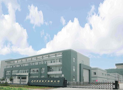
 Building 2, Wanxia Industrial Zone, No. 32, Xiangxing Road, Baoan District, Shenzhen City, Guangdong Province


 Shopping Cart
2
Shopping Cart
2


 Smart Quote